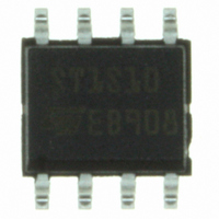
ST1S10PHR STMicroelectronics, ST1S10PHR Datasheet - Page 9

ST1S10PHR
Manufacturer Part Number
ST1S10PHR
Description
IC REG 3A 900KHZ STEPDWN PWRSO-8
Manufacturer
STMicroelectronics
Type
Step-Down (Buck)r
Datasheet
1.ST1S10PUR.pdf
(26 pages)
Specifications of ST1S10PHR
Internal Switch(s)
Yes
Synchronous Rectifier
Yes
Number Of Outputs
1
Voltage - Output
0.8 ~ 15.3 V
Current - Output
3A
Frequency - Switching
900kHz
Voltage - Input
2.5 ~ 18 V
Operating Temperature
-25°C ~ 125°C
Mounting Type
Surface Mount
Package / Case
8-SOIC (3.9mm Width) Exposed Pad, 8-eSOIC. 8-HSOIC
Output Voltage
0.8 V to 15.3 V
Output Current
3 A
Input Voltage
2.5 V to 18 V
Switching Frequency
0.9 MHz
Operating Temperature Range
- 25 C to + 125 C
Mounting Style
SMD/SMT
Duty Cycle (max)
90 %
For Use With
497-8407 - BOARD EVAL STP04CM05/ST1S10497-8216 - BOARD EVAL BASED ON ST1S10497-8229 - BOARD EVAL BASED ON ST1S10
Lead Free Status / RoHS Status
Lead free / RoHS Compliant
Power - Output
-
Lead Free Status / Rohs Status
Lead free / RoHS Compliant
Other names
497-6904-2
ST1S10PHR
ST1S10PHR
Available stocks
Company
Part Number
Manufacturer
Quantity
Price
Company:
Part Number:
ST1S10PHR
Manufacturer:
ST
Quantity:
4 140
Part Number:
ST1S10PHR
Manufacturer:
ST
Quantity:
20 000
ST1S10
5.3
Equation 2
D = (V
where V
drop across the internal PDMOS. The minimum duty cycle (at V
duty cycle (at V
through the input capacitor.
A minimum value of 4.7 µF for the V
suitable in most application conditions. A 10 µF or higher ceramic capacitor for the V
and a 1 µF or higher for the V
impedance or where long wires are needed between the power supply source and the V
pins. The above higher input capacitor values are also recommended in cases where an
output capacitive load is present (47 µF < C
switching peak current drawn from the input capacitor during the start-up transient.
In cases of very high output capacitive loads (C
values shall be modified as described in the OCP and SCP operation
document.
The input ceramic capacitors should have a voltage rating in the range of 1.5 times the
maximum input voltage and be located as close as possible to V
Output capacitor (V
The most important parameters for the output capacitor are the capacitance, the ESR and
the voltage rating. The capacitance and the ESR affect the control loop stability, the output
ripple voltage and transient response of the regulator.
The ripple due to the capacitance can be calculated with the following equation:
Equation 3
V
where F
current, which can be calculated as:
Equation 4
ΔI
where D is the duty cycle.
The ripple due to the ESR is given by:
Equation 5
V
The equations above can be used to define the capacitor selection range, but final values
should be verified by testing an evaluation circuit.
Lower ESR ceramic capacitors are usually recommended to reduce the output ripple
voltage. Capacitors with higher voltage ratings have lower ESR values, resulting in lower
output ripple voltage.
Also, the capacitor ESL value impacts the output ripple voltage, but ceramic capacitors
usually have very low ESL, making ripple voltages due to the ESL negligible. In order to
RIPPLE(C)
RIPPLE
SW
= [(V
OUT
(ESR) = ΔI
S
F
is the PWM switching frequency and ΔI
is the voltage drop across the internal NMOS, and V
IN
+ V
= (0.125 x ΔI
- V
F
) / (V
IN_min
OUT
SW
) / (F
IN
) should be considered in order to determine the max I
x ESR
- V
SW
S
SW
x L)] x D
) / (F
)
IN_A
OUT
Doc ID 13844 Rev 4
S
x C
are recommended in cases of higher power supply source
> 2.5 V)
IN_SW
OUT
)
and a 0.1 µF ceramic capacitor for the V
LOAD
LOAD
SW
< 100 µF), which could impact the
is the inductor peak-to-peak switching
> 100 µF), all input/output capacitor
SW
IN_max
IN
represents the voltage
Application information
pins.
Section 5.8.5
) and the maximum
RMS
flowing
IN_A
of this
IN_SW
are
9/26
IN


