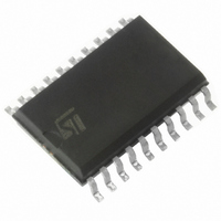
L4979MD013TR STMicroelectronics, L4979MD013TR Datasheet

L4979MD013TR
Specifications of L4979MD013TR
Available stocks
Related parts for L4979MD013TR
L4979MD013TR Summary of contents
Page 1
... The maximum input voltage The max output current is internally limited. Internal temperature protection disables the voltage regulator output. Table 1. Package SO-8 SO-20 Doc ID 10262 Rev 7 L4979D L4979MD SO-20 Device summary Order codes Tube Tape and reel L4979D L4979D013TR L4979MD L4979MD013TR www.st.com 1/22 1 ...
Page 2
Contents 1 Block diagram and pin descriptions . . . . . . . . . . . . . . . . . . . . . . . . . . . . 5 2 Electrical specifications . ...
Page 3
List of tables Table 1. Device summary . . . . . . . . . . . . . . . . . . . . . . . . . . . . . . . . . ...
Page 4
List of figures Figure 1. Block diagram . . . . . . . . . . . . . . . . . . . . . . . . . . . . . . . . . ...
Page 5
Block diagram and pin descriptions Figure 1. Block diagram Table 2. Pin function SO8 SO20 pin number pin number 1 2 5,6,15, Pin name Enable input If high, regulator, watchdog and reset are 1 ...
Page 6
Table 2. Pin function (continued) SO8 SO20 pin number pin number 12, 13, 18, Figure 2. Pins connection (top view) 6/22 Pin name Supply voltage Supply capacitor (e.g. 200 nF) is needed 20 Vs for ...
Page 7
... These are stress ratings only and operation of the device at these or any other conditions above those indicated in the operating sections of this specification is not implied. Exposure to the conditions reported in this section for extended periods may affect device reliability. Refer also to the STMicroelectronics SURE program and other relevant quality documents. Table 3. ...
Page 8
Electrical characteristics Table 5. General Pin Symbol Quiescent current Quiescent current Quiescent ...
Page 9
Table 7. Reset (continued) Pin Symbol Parameter Internal pull- _p_u resistance R V Reset threshold voltage es o_th Reset timing high rhth threshold Reset timing low rlth threshold V I Charge ...
Page 10
Application informations 3.1 Voltage regulator The voltage regulator uses a p-channel MOS transistor as a regulating element. With this structure a low dropout voltage at current up to 150 mA is achieved. The output voltage is regulated up to ...
Page 11
Table 10. Reset time diagram 3.3 Watchdog The watchdog input W reset output R is set to low. The pulse sequence time can be set within a wide range es thorough the external capacitor C the constant current I generated. ...
Page 12
Package and PCB thermal data 4.1 SO-8 thermal data Figure 5. SO-8 PC board 1. Layout condition thickness = 35 mm, Copper areas: from minimum pad lay-out to 2cm Figure 6. R thj-amb 12/22 and Z ...
Page 13
Figure 7. SO-8 thermal impedance junction ambient single pulse Equation 1: pulse calculation formula Z THδ where δ Figure 8. Thermal fitting model of V Doc ID 10262 Rev δ ⋅ Z THtp ...
Page 14
Table 11. SO-8 thermal parameter Area (cm R1 (°C/W) R2 (°C/W) R3 (°C/W) R4 (°C/W) R5 (°C/W) R6 (°C/W) C1 (W.s/°C) C2 (W.s/°C) C3 (W.s/°C) C4 (W.s/°C) C5 (W.s/°C) C6 (W.s/°C) 4.2 SO-20 thermal data Figure 9. SO-20 PC board ...
Page 15
Figure 10 PCB copper area in open box free air condition thj-amb Figure 11. SO-20 thermal impedance junction ambient single pulse Doc ID 10262 Rev 7 15/22 ...
Page 16
Equation 2: pulse calculation formula where δ Figure 12. Thermal fitting model of V Table 12. SO-20 thermal parameter Area (cm R1 (°C/W) R2 (°C/W) R3 (°C/W) R4 (°C/W) R5 (°C/W) R6 (°C/W) C1 (W.s/°C) C2 ...
Page 17
Package information ® 5.1 ECOPACK In order to meet environmental requirements, ST offers these devices in different grades of ® ECOPACK packages, depending on their level of environmental compliance. ECOPACK specifications, grade definitions and product status are available at: ...
Page 18
Table 13. SO-8 mechanical data Symbol Min. A 1.35 A1 0.10 A2 1.10 B 0.33 C 0.19 (1) D 4. 5.80 h 0.25 L 0.40 k ddd 1. Dimensions D does not include mold flash, protrusions ...
Page 19
SO-20 package information Figure 14. SO-20 package dimensions Table 14. SO-20 mechanical data Dim. Min. A 2.35 A1 0.10 B 0.33 C 0.23 (1) D 12. 10.0 h 0.25 L 0.40 k ddd mm Typ. ...
Page 20
Mold flash, protrusions or gate burrs shall not exceed 0.15 mm per side. 20/22 Doc ID 10262 Rev 7 ...
Page 21
Revision history Table 15. Document revision history Date Revision 01-Jun-2004 01-Jul-2004 01-Oct-2004 01-Feb-2006 04-Apr-2011 3 Changed the values of the parameter “Reset timing high/low threshold. Pin Connection SO-20 changed. Changed some textes in the Features 4 and table 2. ...
Page 22
... Information in this document is provided solely in connection with ST products. STMicroelectronics NV and its subsidiaries (“ST”) reserve the right to make changes, corrections, modifications or improvements, to this document, and the products and services described herein at any time, without notice. All ST products are sold pursuant to ST’s terms and conditions of sale. ...


