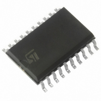
L4972AD STMicroelectronics, L4972AD Datasheet

L4972AD
Specifications of L4972AD
497-4206-5
497-4207-5
Available stocks
Related parts for L4972AD
L4972AD Summary of contents
Page 1
... PowerDIP20 (16+2+2) Table 1. Order Codes Part Number L4972A L4972AD L4972AD013TR uses a DMOS output transistor to obtain very high efficiency and very fast switching times. Features of the L4972 include reset and power fail for micro- processors, feed forward line regulation, soft start, limiting current and thermal protection. The device ...
Page 2
L4972A Table 2. Pin Description N° Pin 1 BOOTSTRAP 2 RESET DELAY 3 RESET OUT 4 RESET INPUT 5, 6 15, GROUND 16 7 FREQUENCY COMPENSATION 8 SOFT START 9 FEEDBACK INPUT 10 SYNC INPUT 11 SUPPLY VOLTAGE 12, 19 ...
Page 3
Table 3. Absolute Maximum Ratings Symbol V Input Voltage 11 V Input Operating Voltage 11 V Output DC Voltage 20 Output Peak Voltage 0.1µ 200kHz I Maximum Output Current 20 V Boostrap Voltage I Boostrap ...
Page 4
L4972A stage. An error signal is produced by comparing the output voltage with the precise 5.1V ± chip reference. This error signal is then compared with the sawtooth oscillator in order to generate frixed fre- quency pulse width ...
Page 5
Figure 6. Limiting Current Function. Figure 7. Reset and Power Fail Functions A B L4972A 5/22 ...
Page 6
L4972A 4 Electrical Characteristcs Table 5. Electrical Characteristcs Refer to the test circuit 25° specified. Symbol Parameter DYNAMIC CHARACTERISTICS V Input Volt. Range (pin 11 Output Voltage o ∆V Line Regulation o ∆V Load ...
Page 7
Table 5. Electrical Characteristcs (continued) Refer to the test circuit 25° specified. Symbol Parameter I Out Leak Current 20L SOFT START (pin 8) I Soft Start Source Current 8 V Output Saturation Voltage 8 ERROR AMPLIFIER ...
Page 8
L4972A Table 5. Electrical Characteristcs (continued) Refer to the test circuit 25° specified. Symbol Parameter V Rising Threshold Voltage 4R V Hysteresis 4H I Input Bias Current 4 Figure 8. TYPICAL PERFORMANCES (using evaluation board) : ...
Page 9
PART LIST R1 = 30KΩ 10KΩ 15KΩ 30KΩ 22Ω 4.7KΩ see table OPTION R9 = 4.7KΩ 1000mF 63V EYF (ROE) ...
Page 10
L4972A Figure 10. P.C. Board and Component Layout of the Circuit of Fig. 8. Figure 11. DC Test Circuits Figure 12. 10/22 ...
Page 11
Figure 13. Figure 14. Figure 15. Figure 16. Quiescent Drain Current vs. Supply Voltage (0% duty cycle - see fig. 12). Figure 17. Quiescent Drain Current vs. Junction Temperature (0% duty cycle). L4972A 11/22 ...
Page 12
L4972A Figure 18. Quiescent Drain Current vs. Duty Cycle. Figure 19. Reference Voltage (pin 13) vs. Vi (see fig. 11). Figure 20. Reference Voltage (pin 13) vs. Junction Temperature (see fig. 11). 12/22 Figure 21. Reference Voltage (pin 14) vs. ...
Page 13
Figure 24. Switching Frequency vs. Input Voltage (see fig. 8). Figure 25. Switching Frequency vs. Junction Temperature (see fig. 8). Figure 26. Switching Frequency vs. R4 (see fig.8). Figure 27. Maximum Duty Cycle vs. Frequency. Figure 28. Supply Voltage Ripple ...
Page 14
L4972A Figure 30. Line Transient Response (see fig. 8). Figure 31. Line Transient Response (see fig. 8). Figure 32. Dropout Voltage between Pin 11 and Pin 20 vs. Current at Pin 20. 14/22 Figure 33. .Dropout Voltage between Pin 11 ...
Page 15
Figure 36. Power Dissipation (device only) vs. Output Voltage. Figure 37. Power Dissipation (device only) vs. Output Voltage Figure 38. Power Dissipation (device only) vs. Output Current Figure 39. Power Dissipation (device only) vs. Output Current Figure 40. Efficiency vs. ...
Page 16
L4972A Figure 42. Rth j-amb vs. Area on Board Heatsink (DIP 16+2+2) Figure 43. Rth j-amb vs. Area on Board Heatsink (SO20) Figure 44. Maximum Allowable Power Dissipation vs. T (Powerdip) amb 16/22 Figure 45. Maximum Allowable Power Dissipation vs. ...
Page 17
Figure 47. 2A – 5.1V Low Cost Application Circuit. Figure 48. A 5.1V/12V Multiple Supply. Note the Synchronization between the L4972A and L4970A. Figure 49. L4972A’s Sync. Example. L4972A 17/22 ...
Page 18
L4972A Figure 50. 1A/24V Multiple Supply. Note the synchronization between the L4972A and L4962 18/22 ...
Page 19
Package Information Figure 51. PowerDIP20 Mechanical Data & Package Dimensions mm DIM. MIN. TYP. MAX. a1 0.51 B 0.85 1.40 b 0.50 b1 0.38 0.50 D 24.80 E 8.80 e 2.54 e3 22.86 F 7.10 I 5.10 L 3.30 ...
Page 20
L4972A Figure 52. SO20 Mechanical Data & Package Dimensions mm DIM. MIN. TYP. MAX. A 2.35 2.65 A1 0.10 0.30 B 0.33 0.51 C 0.23 0.32 (1) 12.60 13. 7.40 7.60 e 1.27 H 10.0 10.65 h 0.25 ...
Page 21
Revision History Table 8. Revision History Date Revision June 2000 May 2005 2 First Issue 3 Modified look & feel layout. Changed the name the Part list to page 9/22. Description of Changes L4972A 21/22 ...
Page 22
... No license is granted by implication or otherwise under any patent or patent rights of STMicroelectronics. Specifications mentioned in this publication are subject to change without notice. This publication supersedes and replaces all information previously supplied. STMicroelectronics products are not authorized for use as critical components in life support devices or systems without express written approval of STMicroelectronics ...


