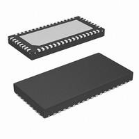
ISL65426HRZ-TS2715 Intersil, ISL65426HRZ-TS2715 Datasheet - Page 7

ISL65426HRZ-TS2715
Manufacturer Part Number
ISL65426HRZ-TS2715
Description
IC REG DUAL SYNC BUCK 50-QFN
Manufacturer
Intersil
Type
Step-Down (Buck)r
Datasheet
1.ISL65426HRZ.pdf
(22 pages)
Specifications of ISL65426HRZ-TS2715
Internal Switch(s)
Yes
Synchronous Rectifier
Yes
Number Of Outputs
2
Voltage - Output
1 ~ 4 V
Current - Output
6A
Frequency - Switching
1MHz
Voltage - Input
3 ~ 5.5 V
Operating Temperature
-10°C ~ 100°C
Mounting Type
Surface Mount
Package / Case
50-VQFN
Lead Free Status / RoHS Status
Lead free / RoHS Compliant
Power - Output
-
Absolute Maximum Ratings
VCC, PVINx, LXx . . . . . . . . . . . . . . . . . . . . . . . . . GND - 0.3V to +6V
FBx, ENx, VxSETx, ISETx, PGOODx . . . . . . . -0.3V to VCC + 0.3V
Recommended Operating Input Range
VCC, PVINx . . . . . . . . . . . . . . . . . . . . . . . . . . . . . . . . . . 3V to +5.5V
CAUTION: Do not operate at or near the maximum ratings listed for extended periods of time. Exposure to such conditions may adversely impact product reliability and
result in failures not covered by warranty.
NOTES:
Electrical Specifications
POWER SUPPLY
Quiescent Supply Current
Shutdown Supply Current
PHASE CONFIGURATION
LX Pull-Down
LX Output Leakage
Minimum Controllable ON-time
OUTPUT VOLTAGE TOLERANCE
Reference Voltage Tolerance
Programmed Output Voltage Tolerance
OSCILLATOR
Accuracy
Maximum LX Pulse Width
Minimum LX Pulse Width
OUTPUT VOLTAGE SELECTION
VxSETx Input High Threshold
VxSETx Pull-down
POWER BLOCKS
ISETx Input High Threshold
ISETx Pull-up
Output Current
Peak Output Current Limit
1. θ
2. For θ
Tech Brief TB379 for details.
JA
is measured in free air with the component mounted on a high effective thermal conductivity test board with “direct attach” features. See
JC
, the “case temp” location is the center of the exposed metal pad on the package underside. See Tech Brief TB379 for details.
PARAMETER
7
Recommended operating conditions, unless otherwise noted. VCC = PVIN = 5.0V,
T
A
= -10°C to +100°C for ISL65426HRZ and T
EN1 = EN2 = EN = VCC = 5V, I
EN1 = EN2 = EN = GND, VCC = PVIN = 5.5V
EN1 = EN2 = EN = GND, VCC = PVIN = 3.3V
LX1, LX3, LX4, LX5, LX6 Only - Configuration Only
Low Level, Single LX Output
High Level, Single LX Output
(Note 3)
T
T
T
T
Per Block; VCC = PVIN = 5.0V; VOUT = 1.8V (Note 3)
Per Block; VCC = PVIN = 3V; VOUT = 1.2V (Note 3)
Per Block
J
J
J
J
= -40°C to +100°C
= 100°C to +125°C
= -40°C to +125°C; No Load
= -40°C to +125°C (Note 4); Full Load
ISL65426
TEST CONDITIONS
Thermal Information
Thermal Resistance
Maximum Junction Temperature (Plastic Package) . . . . . . . +150°C
Maximum Storage Temperature Range . . . . . . . . . .-65°C to +150°C
Ambient Temperature Range (ISL65426HRZ). . . . .-10°C to +100°C
Ambient Temperature Range (ISL65426IRZA) . . . . .-40°C to +85°C
Operating Junction Temperature Range . . . . . . . . .-10°C to +125°C
Pb-free reflow profile . . . . . . . . . . . . . . . . . . . . . . . . . .see link below
OUT1
50 Ld QFN Package (Notes 1, 2). . . . .
http://www.intersil.com/pbfree/Pb-FreeReflow.asp
A
= -40°C to +85°C for ISL65426IRZA. (Note 5)
= I
OUT2
= 0mA
0.594
0.591
MIN
0.8
0.4
0.4
-5
-5
-2
7
7
TYP
125
950
5.4
2.8
0.6
0.6
1.2
1.2
2.0
30
±5
50
10
10
θ
1
1
JA
(°C/W)
23
0.606
0.609
MAX
3.2
1.2
1.5
1.5
0.7
+2
15
15
7
5
5
1
March 25, 2008
θ
JC
UNITS
FN6340.3
2.5
(°C/W)
MHz
mA
mA
mA
mA
µA
µA
µA
µA
ns
ns
ns
%
%
A
V
V
V
V
A
A


