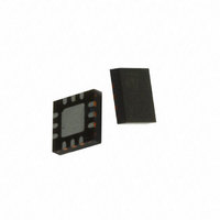
ST2S06D33PQR STMicroelectronics, ST2S06D33PQR Datasheet

ST2S06D33PQR
Specifications of ST2S06D33PQR
Related parts for ST2S06D33PQR
ST2S06D33PQR Summary of contents
Page 1
... ODD applications and, generally, to replace the high current linear solution when Table 1. Device summary Order code (1) ST2S06APQR ST2S06A33PQR ST2S06D33PQR ST2S06BPQR 1. Available on request. March 2008 ST2S06B - ST2S06D33 adjustable step-down switching regulator QFN12L (4x4 mm) the power dissipation may cause a high heating of the application environment ...
Page 2
Contents 1 Diagram . . . . . . . . . . . . . . . . . . . . . . . . . . . . . . . . . . . . . ...
Page 3
Diagram Figure 1. Schematic diagram RESET_OUT * RESET_OUT * Delay Delay HV HV Trimming Trimming FB1 FB1 FB2 FB2 Ref Ref Soft Start Soft Start GND GND * ST2S06A/D ** ST2S06B VI_A VI_A Ref Ref CONTROL CONTROL LOGIC LOGIC ...
Page 4
Pin configuration Figure 2. Pin connections (top view) Table 2. Pin description Pin n° ST2S06A/D ST2S06B FB2 3 GND2 4 SW2 5 VIN_SW 6 SW1 7 GND1 8 FB1/OUT1 9 Reset_out VIN_A 12 ...
Page 5
Maximum ratings Table 3. Absolute maximum ratings Symbol V Positive power supply voltage IN_SW V Positive power supply voltage IN_A V Inhibit voltage INH SWITCH voltage Max. voltage of output pin V /V Feedback voltage/output voltage FB1 ...
Page 6
Electrical characteristics Table 6. Electrical characteristics for ST2S06A ( µ 3.3 µ values are referred to 25 °C Symbol Parameter FB Feedback voltage 1 pin ...
Page 7
Table 7. Electrical characteristics for ST2S06A33 ( 4.7 µ specified. Typical values are referred to 25 °C Symbol Parameter OUT Output feedback pin 1 FB Feedback voltage pin bias current ...
Page 8
Table 8. Electrical characteristics for ST2S06D33 ( 4.7 µ specified. Typical values are referred to 25 °C Symbol Parameter OUT Output feedback pin 1 FB Feedback voltage pin bias current ...
Page 9
Table 9. Electrical characteristics for ST2S06B ( µ 3.3 µ values are referred to 25 °C Symbol Parameter FB Feedback voltage 1 pin bias current FB1,2 ...
Page 10
Typical performance characteristics Figure 3. Feedback voltage 1 vs. temperature (ST2S06B) 0.82 0. =5V, V =5V, V connected to V connected FB1 FB1 =NO LOAD =NO LOAD ...
Page 11
Figure 9. Switching frequency vs. temperature (ST2S06B) 1.9 1.9 1.8 1.8 1.7 1.7 1.6 1.6 1.5 1.5 1.4 1.4 1.3 1.3 1.2 1.2 1.1 1.1 -50 -50 -25 - Temperature [°C] Temperature [°C] Figure ...
Page 12
Figure 15. Delay time vs. temperature (ST2S06A) 100 100 Rising from Rising from ...
Page 13
Figure 21. Start-up transient (ST2S06B from 0V to 5V, I =1A, Output Voltage=1. Figure 22. Inhibit transient (ST2S06B) V INH from 0V to 2V, ...
Page 14
Typical application Figure 23. Application circuit for ST2S06A VIN_A VIN_A VIN_SW VIN_SW NC NC Reset_Out Reset_Out GND1 GND1 C1 C1 4.7µF 4.7µF Figure 24. Application circuit for ST2S06B VIN_A VIN_A VIN_SW ...
Page 15
Application information The ST2S06 represents a series of dual adjustable current mode PWM step-down DC-DC converters with an internal 0.5 A power switch, packaged in a QFN12L (4x4 mm complete 0.5 A switching regulator with internal ...
Page 16
Package mechanical data In order to meet environmental requirements, ST offers these devices in ECOPACK packages. These packages have a lead-free second level interconnect. The category of second Level Interconnect is marked on the package and on the inner ...
Page 17
QFN12L (4x4) mechanical data mm. Dim. Min. Typ. A 0.80 0.90 A1 0.02 A3 0.20 b 0.25 0.30 D 3.90 4.00 D2 2.00 2.15 E 3.90 4.00 E2 2.00 2.15 e 0.80 L 0.45 0.55 inch. Max. Min. Typ. 1.00 ...
Page 18
Tape & reel QFNxx/DFNxx (4x4) mechanical data Dim. Min 12 18/21 mm. Typ. Max. Min. 330 13.2 0.504 0.795 101 3.898 14.4 4.35 4.35 1 inch. ...
Page 19
Figure 26. QFN12L (4x4 mm) footprint recommended data 19/21 ...
Page 20
Revision history Table 10. Document revision history Date Revision 3-Sep-2007 1 21-Jan-2008 2 18-Mar-2008 3 20/21 Changes Initial release. Added root part number ST2S06D33. Modified: Table 2 on page 4 . ...
Page 21
... Information in this document is provided solely in connection with ST products. STMicroelectronics NV and its subsidiaries (“ST”) reserve the right to make changes, corrections, modifications or improvements, to this document, and the products and services described herein at any time, without notice. All ST products are sold pursuant to ST’s terms and conditions of sale. ...


