HCPL-0701-000E Avago Technologies US Inc., HCPL-0701-000E Datasheet
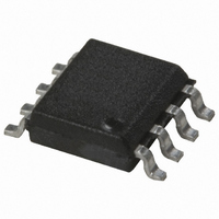
OPTOCOUPLR DARL-OUT 100KBD 8SOIC

HCPL-0701-000E

Manufacturer Part Number
HCPL-0701-000E
Description
OPTOCOUPLR DARL-OUT 100KBD 8SOIC
Manufacturer
Avago Technologies US Inc.
Type
Logicr
Datasheets

Specifications of HCPL-0701-000E

Input Type
DC
Package / Case
8-SOIC (0.154", 3.90mm Width)
Voltage - Isolation
3750Vrms
Number Of Channels
1, Unidirectional
Current - Output / Channel
60mA
Data Rate
100KBd
Propagation Delay High - Low @ If
5µs @ 500µA
Current - Dc Forward (if)
20mA
Output Type
Open Collector
Mounting Type
Surface Mount
Isolation Voltage
3750 Vrms
Maximum Continuous Output Current
60 mA
Maximum Forward Diode Current
20 mA
Minimum Forward Diode Voltage
1.25 V
Output Device
Darlington With Base
Configuration
1 Channel
Current Transfer Ratio
5000 %
Maximum Baud Rate
100 KBps
Maximum Forward Diode Voltage
1.7 V
Maximum Reverse Diode Voltage
5 V
Maximum Input Diode Current
20 mA
Maximum Power Dissipation
135 mW
Maximum Operating Temperature
+ 70 C
Minimum Operating Temperature
0 C
Number Of Elements
1
Reverse Breakdown Voltage
5V
Forward Voltage
1.7V
Forward Current
20mA
Package Type
SOIC
Collector Current (dc) (max)
60mA
Power Dissipation
135mW
Pin Count
8
Mounting
Surface Mount
Operating Temp Range
0C to 70C
Operating Temperature Classification
Commercial
No. Of Channels
1
Optocoupler Output Type
Photodarlington
Input Current
12mA
Output Voltage
18V
Opto Case Style
SOIC
No. Of Pins
8
Ctr Max
5000%
Ctr Min
400%
Rohs Compliant
Yes
Lead Free Status / RoHS Status
Lead free / RoHS Compliant
Lead Free Status / RoHS Status
Lead free / RoHS Compliant, Lead free / RoHS Compliant
Other names
516-1637-5

Available stocks

Company
Part Number
Manufacturer
Quantity
Price
Part Number:
HCPL-0701-000E
Manufacturer:
AVAGO
Quantity:
40 000
Part Number:
HCPL-0701-000E
Manufacturer:
AVAGO
Quantity:
20 000
Company:
Part Number:
HCPL-0701-000E
Quantity:
315
6N139, 6N138, HCPL-0701, HCPL-0700,
HCNW139, HCNW-138
Low Input Current, High Gain Optocouplers
Data Sheet
Description
These high gain series couplers use a Light Emitting
Diode and an integrated high gain photodetec tor to
provide extremely high current transfer ratio between
input and output. Separate pins for the photodiode
and output stage result in TTL compatible saturation
voltages and high speed operation. Where desired the
V
conven tional photodarlington operation. A base
access terminal allows a gain bandwidth adjustment to
be made.
The 6N139, HCPL-0701, and CNW139 are for use in CMOS,
LSTTL or other low power appli ca tions. A 400% mini-
mum current transfer ratio is guaranteed over 0 to 70°C
operating range for only 0.5 mA of LED current.
The 6N138, HCPL-0700, and HCNW138 are designed for
use mainly in TTL applications. Current Transfer Ratio
(CTR) is 300% minimum over 0 to 70°C for an LED current
of 1.6 mA (1 TTL Unit load ). A 300% minimum CTR
enables operation with 1 TTL Load using a 2.2 kΩ
pull-up resistor.
Functional Diagram
*5000 V rms/1 minute rating is for HCNW139/138 and Option 020
(6N139/138) products only.
A 0.1 µF bypass capacitor connected between pins 8 and 5 is
recommended.
CC
RoHS 6 fully compliant options available;
-xxxE denotes a lead-free product
CATHODE
and V
ANODE
NC
NC
O
Lead (Pb) Free
RoHS 6 fully
compliant
1
2
3
4
terminals may be tied together to achieve
CAUTION: It is advised that normal static precautions be taken in handling and assembly
of this component to prevent damage and/or degradation which may be induced by ESD.
6N139 Functional Diagram
8
7
6
5
V
V
V
GND
CC
B
O
LED
OFF
TRUTH TABLE
ON
HIGH
LOW
V
O
Features
• High current transfer ratio – 2000% typical (4500 %
• Low input current requirements – 0.5 mA
• TTL compatible output – 0.1 V V
• Performance guaranteed over temperature 0°C
• Base access allows gain bandwidth adjustment
• High output current – 60 mA
• Safetyapproval
• Available in 8-Pin DIP or SOIC-8 footprint or widebody
• MIL-PRF-38534 hermetic version available
Applications
• Ground isolate most logic families – TTL/TTL, CMOS/
• Low input current line receiver
• High voltage insulation (HCNW139/138)
• EIA RS-232C line receiver
• Telephone ring detector
• 117 V ac line voltage status indicator – low input
• Low power systems – ground isolation
typical for HCNW139/138)
to 70°C
UL recognized – 3750 V rms for 1 minute and 5000 V
CSA approved
IEC/EN/DIN EN 60747-5-2 approved with V
package
(HCPL-5700/1)
TTL, CMOS/CMOS, LSTTL/TTL, CMOS/LSTTL
power dissipation
V
rms* for 1 minute per UL 1577
peak
for HCNW139 and HCNW138
OL
typical
IORM
= 1414

Related parts for HCPL-0701-000E

HCPL-0701-000E Summary of contents

Page 1

... A base access terminal allows a gain bandwidth adjustment to be made. The 6N139, HCPL-0701, and CNW139 are for use in CMOS, LSTTL or other low power appli ca tions. A 400% mini- mum current transfer ratio is guaranteed over 0 to 70°C operating range for only 0 LED current. ...

Page 2

... Selection for lower input current down to 250 µA is available upon request. The HCPL-0701 and HCPL-0700 are surface mount devices packaged in an industry standard SOIC-8 footprint. The SOIC-8 does not require “through holes” PCB. This package occupies approximately one-third the footprint area of the standard dual-in-line package. The ...

Page 3

... Ordering Information 6N138, 6N139, HCPL-0700 and HCPL-0701 are UL Recognized with 3750 Vrms for 1 minute per UL1577 and are approved under CSA Component Acceptance Notice #5, File CA 88324. Option Part RoHS non RoHS Number Compliant Compliant Package -000E no option 300 mil DIP-8 -300E ...

Page 4

Package Outline Drawings 8-Pin DIP Package (6N139/6N138)** 9.65 ± 0.25 (0.380 ± 0.010 TYPE NUMBER A XXXXZ YYWW 1.19 (0.047) MAX. 3.56 ± 0.13 (0.140 ± 0.005) 1.080 ± 0.320 (0.043 ± 0.013) **JEDEC ...

Page 5

... Small Outline SO-8 Package (HCPL-0701/HCPL-0700 3.937 ± 0.127 (0.155 ± 0.005 PIN ONE 0.406 ± 0.076 (0.016 ± 0.003) * 5.080 ± 0.127 (0.200 ± 0.005) 3.175 ± 0.127 (0.125 ± 0.005) * TOTAL PACKAGE LENGTH (INCLUSIVE OF MOLD FLASH) 5.207 ± 0.254 (0.205 ± 0.010) DIMENSIONS IN MILLIMETERS (INCHES) ...

Page 6

Widebody DIP Package with Gull Wing Surface Mount Option 300 (HCNW139/HCNW138) 11.23 ± 0.15 (0.442 ± 0.006 1.80 ± 0.15 (0.071 ± 0.006) 2.54 (0.100) BSC DIMENSIONS IN MILLIMETERS (INCHES). LEAD COPLANARITY = ...

Page 7

... PREHEAT 60 to 180 SEC °C to PEAK TIME Regulatory Information The 6N139/138, HCNW139/138, and HCPL-0701/0700 have been approved by the following organizations: UL Recognized under UL 1577, Component Recognition Program, File E55361. CSA Approved under CSA Component Acceptance Notice #5, File CA 88324. Insulation and Safety Related Specifications ...

Page 8

IEC/EN/DIN EN 60747-5-2 Insulation Related Characteristics (HCNW139 and HCNW138) Description Installation Classification per DIN VDE 0110/1.89, Table 1 for rated mains voltage ≤600 V rms for rated mains voltage ≤1000 V rms Climatic Classification Pollution Degree (DIN VDE 0110/1.89) Maximum ...

Page 9

... Output Current (Pin 6) Emitter Base Reverse Voltage (Pin 5-7) Supply Voltage and Output Voltage (6N139, HCPL-0701, HCNW139) Supply Voltage and Output Voltage (6N138, HCPL-0700, HCNW138) Output Power Dissipation Total Power Dissipation Lead Solder Temperature (for Through Hole Devices) Reflow Temperature Profile (for SOIC-8 and Option #300) *JEDEC Registered Data for 6N139 and 6N138 ...

Page 10

... HCPL-0701 HCNW139 6N138 HCPL-0700 HCNW138 Logic High I 6N139 OH Output Current HCPL-0701 HCNW139 6N138 HCPL-0700 HCNW138 Logic Low Supply I 6N138/139 CCL Current HCPL-0701/ 0700 HCNW139 HCNW138 Logic High I 6N138/139 CCH Supply Current HCPL-0701/ 0700 HCNW139 HCNW138 Input Forward V 6N138 F Voltage 6N139 HCPL-0701 ...

Page 11

... HCPL-0701 to Logic Low HCNW139 at Output 6N139 HCPL-0701 HCNW139 6N138 HCPL-0700 HCNW138 Propagation t 6N139 PLH Delay Time HCPL-0701 to Logic High HCNW139 at Output 6N139 HCPL-0701 HCNW139 6N138 HCPL-0700 HCNW138 Common Mode | Transient Immunity at Logic High Output Common Mode | Transient Immunity at Logic Low Output *JEDEC Registered Data for 6N139 and 6N138 ...

Page 12

Package Characteristics Parameter Input-Output Momentary Withstand Voltage† Option 020 HCNW139 HCNW138 Resistance (Input-Output) Capacitance (Input-Output) **All typicals 25°C, unless otherwise noted. A †The Input-Output Momentary Withstand Voltage is a dielectric voltage rating that should not be interpreted ...

Page 13

25° 1.0 2.0 V – OUTPUT VOLTAGE – Figure 1. 6N138/6N139 DC transfer character- istics 6N1390 fig ...

Page 14

0 0.3 0.2 0 – FORWARD CURRENT F Figure 10. Logic low supply current vs. forward ...

Related keywords