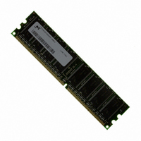
MT8VDDT6464AY-40BF4 Micron Technology Inc, MT8VDDT6464AY-40BF4 Datasheet - Page 18

MT8VDDT6464AY-40BF4
Manufacturer Part Number
MT8VDDT6464AY-40BF4
Description
MODULE DDR SDRAM 512MB 184-DIMM
Manufacturer
Micron Technology Inc
Datasheet
1.MT8VDDT6464AY-40BF4.pdf
(26 pages)
Specifications of MT8VDDT6464AY-40BF4
Memory Type
DDR SDRAM
Memory Size
512MB
Speed
400MT/s
Package / Case
184-DIMM
Lead Free Status / RoHS Status
Lead free / RoHS Compliant
Other names
557-1232
MT8VDDT6464AY-40BF4
MT8VDDT6464AY-40BF4
Figure 6:
PDF: 09005aef80a43556, Source: 09005aef80a43534
DDA8C16_32_64x64AG_2.fm - Rev. E 4/06 EN
Pull-Up Characteristics
21. The voltage levels used are derived from a minimum V
22. V
23. During initialization, V
24. For -40B modules, I
25. Random addressing changing and 50 percent of data changing at every transfer.
26. Random addressing changing and 100 percent of data changing at every transfer.
27. CKE must be active (HIGH) during the entire time a refresh command is executed.
28. I
29. Leakage number reflects the worst case leakage possible through the module pin, not
30. When an input signal is HIGH or LOW, it is defined as a steady state logic high or low.
31. This is the DC voltage supplied at the DRAM and is inclusive of all noise up to 20 MHz.
-100
-120
-140
-160
-180
-200
-20
-40
-60
-80
load. In practice, the voltage levels obtained from a properly terminated bus will pro-
vide significantly different voltage values.
Alternatively, V
provided a minimum of 42Ω of series resistance is used between the V
the input pin.
That is, from the time the AUTO REFRESH command is registered, CKE must be
active at each rising clock edge, until
I
remain stable. Although I
what each memory device contributes.
Any noise above 20 MHz at the DRAM device generated from any source other than
that of the DRAM itself may not exceed the DC voltage range of 2.6V ±100mV.
DD
DD
0
DD
0.0
2N specifies the DQ, DQS, and DM to be driven to a valid high or low logic level.
2Q is similar to I
and V
128MB, 256MB, 512MB (x64, SR): PC3200 184-Pin DDR UDIMM
DD
0.5
Q must track each other.
TT
may be 1.35V maximum during power up, even if V
DD
DD
1.0
V
3N is specified to be 35mA per DDR SDRAM device at 100 MHz.
2
DD
DD
F
Q - V
except I
DD
Q, V
18
OUT
2F, I
(V)
TT
1.5
DD
, and V
DD
2N, and I
2Q specifies the address and control inputs to
Micron Technology, Inc., reserves the right to change products or specifications without notice.
t
RFC has been satisfied.
REF
2.0
must be equal to or less than V
DD
2Q are similar, I
2.5
DD
level and the referenced test
©2005 Micron Technology, Inc. All rights reserved.
DD
2F is “worst case.”
DD
TT
/V
supply and
DD
DD
Q are 0V,
+ 0.3V.
Notes


