MT16HTF12864HY-53ED3 Micron Technology Inc, MT16HTF12864HY-53ED3 Datasheet
MT16HTF12864HY-53ED3
Specifications of MT16HTF12864HY-53ED3


Related parts for MT16HTF12864HY-53ED3


MT16HTF12864HY-53ED3 Summary of contents
Page 1
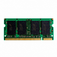
DDR2 SDRAM SODIMM MT16HTF12864H(I) – 1GB MT16HTF25664H(I) – 2GB For component data sheets, refer to Micron’s Web site: Features • 200-pin, small outline, dual in-line memory module (SODIMM) • Fast data transfer rates: PC2-3200, PC2-4200, PC2-5300, or PC2-6400. • 1GB ...
Page 2
... Part Numbers and Timing Parameters – 1GB Modules Base device: MT47H64M8, 512Mb DDR2 SDRAM 1 Part Number MT16HTF12864H(I)Y-80E__ MT16HTF12864H(I)Y-800__ MT16HTF12864H(I)Y-667__ MT16HTF12864H(I)Y-53E__ MT16HTF12864H(I)Y-40E__ Table 4: Part Numbers and Timing Parameters – 2GB Modules Base device: MT47H128M8, 1Gb DDR2 SDRAM 1 Part Number MT16HTF25664H(I)Y-80E__ MT16HTF25664H(I)Y-800__ MT16HTF25664H(I)Y-667__ MT16HTF25664H(I)Y-53E__ MT16HTF25664H(I)Y-40E__ Notes: 1 ...
Page 3
Module Pin Assignments and Descriptions Table 5: Pin Assignments 200-Pin SODIMM Front Pin Symbol Pin Symbol Pin Symbol Pin Symbol DQS2 101 REF 103 DQ0 55 DQ18 105 A10/AP 155 ...
Page 4
Table 6: Pin Descriptions Symbol Type ODT0, ODT1 Input On-die termination: ODT (registered HIGH) enables termination resistance internal to the DDR2 SDRAM. When enabled, ODT is only applied to each of the following pins: DQ, DQS, DQS#, and DM. The ...
Page 5
Figure 2: Functional Block Diagram 10Ω S1# 10Ω S0# DQS0# DQS0 DM0 DM CS# DQ DQ0 DQ DQ1 DQ DQ2 DQ U2 DQ3 DQ DQ4 DQ DQ5 DQ DQ6 DQ DQ7 DQ DQS1# DQS1 DM1 DM CS# DQ DQ8 DQ ...
Page 6
... DQS is edge-aligned with data for reads and center-aligned with data for writes. DDR2 SDRAM modules operate from a differential clock (CK and CK#); the crossing of CK going HIGH and CK# going LOW will be referred to as the positive edge of CK. ...
Page 7
... Simulations can then render a considerably more accurate result. JEDEC modules are now designed using simulations to close timing budgets. AC Timing and Operating Conditions Recommended AC operating conditions are given in the DDR2 component data sheets, available on Micron’ ...
Page 8
Table 9: DDR2 I Specifications and Conditions – 1GB DD Values shown for DDR2 SDRAM components only Parameter/Condition Operating one bank active-precharge current RAS = RAS MIN ( commands; ...
Page 9
Table 10: DDR2 I Specifications and Conditions – 2GB (die revision A) DD Values shown for DDR2 SDRAM components only Parameter/Condition Operating one bank active-precharge current RAS = RAS MIN (I ...
Page 10
Table 11: DDR2 I Specifications and Conditions – 2GB (die revision E) DD Values shown for DDR2 SDRAM components only Parameter/Condition Operating one bank active-precharge current RAS = RAS MIN (I ...
Page 11
Serial Presence-Detect Table 12: Serial Presence-Detect EEPROM DC Operating Conditions All voltages referenced to V Parameter/Condition Supply voltage Input high voltage: Logic 1; All inputs Input low voltage: Logic 0; All inputs Output low voltage 3mA OUT Input ...
Page 12
Table 14: Serial Presence-Detect Matrix “1”/“0”: Serial Data, “driven to HIGH”/“driven to LOW”; table notes located on page 14 Byte Description 0 Number of SPD bytes used by Micron 1 Total Number of bytes in SPD device 2 Fundamental memory ...
Page 13
Table 14: Serial Presence-Detect Matrix “1”/“0”: Serial Data, “driven to HIGH”/“driven to LOW”; table notes located on page 14 Byte Description 27 Minimum row precharge time, 28 Minimum row active to row active, 29 Minimum RAS#-to-CAS# delay, 30 Minimum RAS# ...
Page 14
Table 14: Serial Presence-Detect Matrix “1”/“0”: Serial Data, “driven to HIGH”/“driven to LOW”; table notes located on page 14 Byte Description 63 Checksum for bytes 0–62 64 Manufacturer’s JEDEC ID code 65–71 Manufacturer’s JEDEC ID code 72 Manufacturing location 73–90 ...
Page 15
Module Dimensions Figure 3: 200-pin DDR2 SODIMM Module Dimensions 2.0 (0.079) R (2X) U2 1.80 (0.071) (2X) U6 6.00 (0.236) TYP PIN 1 2.00 (0.079) TYP 16.25 (0.64) TYP U11 U15 3.50 (0.138) TYP PIN 200 Notes: 1. All dimensions ...
Page 16
Revision History Rev. B, Released (No Mark ...