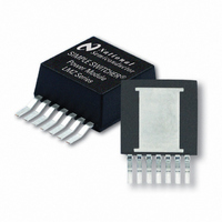
LMZ10504TZ-ADJ/NOPB National Semiconductor, LMZ10504TZ-ADJ/NOPB Datasheet - Page 10

LMZ10504TZ-ADJ/NOPB
Manufacturer Part Number
LMZ10504TZ-ADJ/NOPB
Description
IC BUCK SYNC ADJ 4A TO-PMOD-7
Manufacturer
National Semiconductor
Series
SIMPLE SWITCHER®r
Type
Point of Load (POL) Non-Isolated with UVLOr
Datasheet
1.LMZ10504TZ-ADJNOPB.pdf
(22 pages)
Specifications of LMZ10504TZ-ADJ/NOPB
Output
0.8 ~ 5 V
Number Of Outputs
1
Power (watts)
20W
Mounting Type
Surface Mount
Voltage - Input
2.95 ~ 5.5 V
Package / Case
TO-PMOD-7, Power Module
1st Output
0.8 ~ 5 VDC @ 4A
Size / Dimension
0.40" L x 0.54" W x 0.18" H (10.16mm x 13.77mm x 4.57mm)
Power (watts) - Rated
20W
Operating Temperature
-40°C ~ 125°C
Efficiency
96%
Approvals
EN
Lead Free Status / RoHS Status
Lead free / RoHS Compliant
3rd Output
-
2nd Output
-
Other names
LMZ10504TZ-ADJTR
Available stocks
Company
Part Number
Manufacturer
Quantity
Price
Company:
Part Number:
LMZ10504TZ-ADJ/NOPB
Manufacturer:
NS
Quantity:
1 000
www.national.com
Output Voltage Setting
A resistor divider network from V
the desired output voltage as follows:
R
R
are normally selected as 0.5% or 1% tolerance. Higher accu-
racy resistors such as 0.1% are also available.
The feedback voltage (at V
-2.5% / +2.5% over temperature and over line and load reg-
ulation. Additionally, the LMZ10504 contains error nulling
circuitry to substantially eliminate the feedback voltage vari-
ation over temperature as well as the long term aging effects
of the internal amplifiers. In addition the zero nulling circuit
dramatically reduces the 1/f noise of the bandgap amplifier
and reference. The manifestation of this circuit action is that
the duty cycle will have two slightly different but distinct op-
erating points, each evident every other switching cycle.
Loop Compensation
The LMZ10504 preserves flexibility by integrating the control
components around the internal error amplifier while utilizing
three small external compensation components from V
FB. An integrated type II (two pole, one zero) voltage-mode
compensation network is featured. To ensure stability, an ex-
ternal resistor and small value capacitor can be added across
the upper feedback resistor as a pole-zero pair to complete a
type III (three pole, two zero) compensation network. The
compensation components recommended in
type III compensation at an optimal control loop performance.
The typical phase margin is 45° with a bandwidth of 80 kHz.
Calculated output capacitance values not listed in
should be verified before designing into production. A detailed
application note is available to provide verification support,
AN-2013. In general, calculated output capacitance values
below the suggested value will have reduced phase margin
and higher control loop bandwidth. Output capacitance val-
ues above the suggested values will experience a lower
bandwidth and increased phase margin. Higher bandwidth is
associated with faster system response to sudden changes
such as load transients. Phase margin changes the charac-
teristics of the response. Lower phase margin is associated
with underdamped ringing and higher phase margin is asso-
ciated with overdamped response. Losing all phase margin
will cause the system to be unstable; an optimized area of
C
fbt
fbb
O
100
100
100
150
330
470
22
47
47
47
is defined based on the voltage loop requirements and
is then selected for the desired output voltage. Resistors
(µF)
Voltage (V), R
10.0, < 5
6.3, < 5
6.3, < 5
6.3, < 5
6.3, < 5
6.3, 50
6.3, 25
6.3, 18
6.3, 18
6.3, 23
OUT
ESR
= 2.5V) is accurate to within
OUT
(mΩ)
to the FB pin determines
TABLE 1. Recommended Output Filter Capacitors
Organic Polymer
Organic Polymer
Organic Polymer
Niobium Oxide
Ceramic, X5R
Ceramic, X5R
Ceramic, X5R
Ceramic, X5R
Ceramic, X5R
Table 2
Tantalum
Make
Table 2
provide
OUT
to
10
Manufacturer
operation is 30° to 60° of phase margin, with a bandwidth of
100 kHz ±20 kHz.
Note: In the special case where the output voltage is 0.8V, it is recom-
TABLE 2. LMZ10504 Compensation Component Values
Sanyo
Sanyo
Sanyo
TDK
TDK
TDK
TDK
TDK
AVX
AVX
V
(V)
5.0
3.3
IN
mended to remove R
compensation.
C
O
100
150
150
150
220
220
100
150
150
150
220
220
22
47
22
47
(µF)
TPSD157M006#0050
NOME37M006#0023
C3225X5R1A476M
C3216X5R0J226M
C3216X5R0J476M
C3225X5R0J476M
C3225X5R0J107M
6TPE100MPB2
6TPE150MIC2
Part Number
6TPE330MIL
ESR (mΩ)
Min
10
26
15
31
10
26
15
31
2
2
1
1
2
2
1
1
fbb
and keep R
Max
20
20
10
25
50
30
60
20
20
10
25
50
30
60
5
5
fbt
(kΩ)
82.5
63.4
63.4
44.2
63.4
76.8
76.8
49.9
40.2
43.2
49.9
40.2
48.7
R
200
124
118
, R
fbt
comp
D3L, 7.3 x 4.3 x 2.8 mm
C2, 6.0 x 3.2 x 1.8 mm
B2, 3.5 x 2.8 x 1.9 mm
D, 7.5 x 4.3 x 2.9 mm
E, 7.3 x 4.3 x 4.1 mm
, and C
C
(pF)
120
180
220
220
220
220
180
330
330
270
390
330
comp
27
56
39
82
Case Size
comp
1206
1206
1210
1210
1210
30088248
R
for a type III
(kΩ)
1.21
16.5
23.7
23.7
57.6
9.09
8.45
4.12
11.5
25.5
15.4
35.7
1.5
1.4
2.0
comp
1


