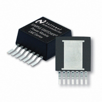
LMZ10504TZ-ADJ/NOPB National Semiconductor, LMZ10504TZ-ADJ/NOPB Datasheet - Page 4

LMZ10504TZ-ADJ/NOPB
Manufacturer Part Number
LMZ10504TZ-ADJ/NOPB
Description
IC BUCK SYNC ADJ 4A TO-PMOD-7
Manufacturer
National Semiconductor
Series
SIMPLE SWITCHER®r
Type
Point of Load (POL) Non-Isolated with UVLOr
Datasheet
1.LMZ10504TZ-ADJNOPB.pdf
(22 pages)
Specifications of LMZ10504TZ-ADJ/NOPB
Output
0.8 ~ 5 V
Number Of Outputs
1
Power (watts)
20W
Mounting Type
Surface Mount
Voltage - Input
2.95 ~ 5.5 V
Package / Case
TO-PMOD-7, Power Module
1st Output
0.8 ~ 5 VDC @ 4A
Size / Dimension
0.40" L x 0.54" W x 0.18" H (10.16mm x 13.77mm x 4.57mm)
Power (watts) - Rated
20W
Operating Temperature
-40°C ~ 125°C
Efficiency
96%
Approvals
EN
Lead Free Status / RoHS Status
Lead free / RoHS Compliant
3rd Output
-
2nd Output
-
Other names
LMZ10504TZ-ADJTR
Available stocks
Company
Part Number
Manufacturer
Quantity
Price
Company:
Part Number:
LMZ10504TZ-ADJ/NOPB
Manufacturer:
NS
Quantity:
1 000
www.national.com
PERFORMANCE PARAMETERS
Efficiency
Electrical Characteristics
apply over the operating junction temperature range T
test, design, or statistical correlation. Typical values represent the most likely parametric norm at T
reference purposes only. V
Note 1: θ
dissipation. Refer to
Note 2: EN 55022:2006, +A1:2007, FCC Part 15 Subpart B: 2007. See
Note 3: Absolute Maximum Ratings are limits beyond which damage to the device may occur. Operating Ratings are conditions under which operation of the
device is intended to be functional. For guaranteed specifications and test conditions, see the Electrical Characteristics.
Note 4: The human body model is a 100 pF capacitor discharged through a 1.5 kΩ resistor into each pin. Test method is per JESD22-AI14S.
Note 5: Min and Max limits are 100% production tested at an ambient temperature (T
through correlation using Statistical Quality Control (SQC) methods. Limits are used to calculate National’s Average Outgoing Quality Level (AOQL).
Note 6: Typical numbers are at 25°C and represent the most likely parametric norm.
ΔV
ΔV
ΔV
ΔV
Symbol
OUT
OUT
ΔV
ΔV
FB
FB
η
η
η
η
OUT
OUT
/ V
/ V
/ V
/ V
JA
measured on a 2.25” x 2.25” (5.8 cm x 5.8 cm) four layer board, with one ounce copper, thirty six 10mil thermal vias, no air flow, and 1W power
FB
OUT
FB
OUT
PCB Layout Diagrams
Parameter
Output Voltage Ripple
Output Voltage Ripple
Feedback Voltage Line Regulation
Output Voltage Line Regulation
Feedback Voltage Load Regulation
Output Voltage Load Regulation
Peak Efficiency (1A) V
Peak Efficiency (1A) V
Full Load Efficiency (4A) V
Full Load Efficiency (4A) V
IN
= V
EN
or Evaluation Board Application Note: AN-2022.
= 3.3V, unless otherwise indicated in the conditions column.
IN
IN
= 5V
= 3.3V
Specifications with standard typeface are for T
IN
IN
= 5V
= 3.3V
J
of -40°C to 125°C. Minimum and maximum limits are guaranteed through
Table 9
Conditions
Refer to
V
Bandwidth Limit = 2 MHz
Refer to
Bandwidth Limit = 20 MHz
ΔV
I
ΔV
I
I
I
V
V
V
V
V
V
V
V
V
V
V
V
V
V
V
V
V
V
V
V
V
V
V
OUT
OUT
OUT
OUT
OUT
OUT
OUT
OUT
OUT
OUT
OUT
OUT
OUT
OUT
OUT
OUT
OUT
OUT
OUT
OUT
OUT
OUT
OUT
OUT
OUT
OUT
OUT
OUT
IN
IN
4
and layout for information on device under test.
= 0A
= 0A, V
= 0A to 4A
= 0A to 4A
= 2.95V to 5.5V
= 2.95V to 5.5V
= 2.5V
= 2.5V
= 3.3V
= 2.5V
= 1.8V
= 1.5V
= 1.2V
= 0.8V
= 2.5V
= 1.8V
= 1.5V
= 1.2V
= 0.8V
= 3.3V
= 2.5V
= 1.8V
= 1.5V
= 1.2V
= 0.8V
= 2.5V
= 1.8V
= 1.5V
= 1.2V
= 0.8V
Table 3
Table 5
A
) of 25°C. Limits over the operating temperature range are guaranteed
OUT
= 2.5V
(Note
Min
J
= 25°C only; limits in bold face type
5)
J
= 25°C, and are provided for
(Note
0.04
0.04
0.25
0.25
96.1
94.8
93.1
90.4
86.8
95.7
94.1
93.0
91.6
88.3
94.1
92.4
90.0
88.3
86.1
80.8
91.4
90.0
87.2
84.9
79.3
Typ
10
92
5
6)
(Note
Max
5)
mV
mV
Units
%
%
%
%
%
%
%
%
pk-pk
pk-pk


