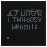
LTM4605IV#PBF Linear Technology, LTM4605IV#PBF Datasheet - Page 10

LTM4605IV#PBF
Manufacturer Part Number
LTM4605IV#PBF
Description
IC DC/DC UMODULE 5A 141-LGA
Manufacturer
Linear Technology
Series
µModuler
Type
Point of Load (POL) Non-Isolatedr
Datasheet
1.LTM4605EVPBF.pdf
(26 pages)
Specifications of LTM4605IV#PBF
Design Resources
LTM4605 Spice Model
Output
0.8 ~ 16 V
Number Of Outputs
1
Power (watts)
80W
Mounting Type
Surface Mount
Voltage - Input
4.5 ~ 20V
Package / Case
141-LGA
1st Output
0.8 ~ 16 VDC @ 5A
Size / Dimension
0.59" L x 0.59" W x 0.11" H (15mm x 15mm x 2.8mm)
Power (watts) - Rated
80W
Operating Temperature
-40°C ~ 85°C
Efficiency
98%
Dc To Dc Converter Type
Non-Inverting/Inverting/Step Up/Step Down
Pin Count
141
Input Voltage
20V
Output Voltage
0.8 to 16V
Switching Freq
170 TO 440KHz
Output Current
12/5A
Package Type
LGA
Output Type
Adjustable
Switching Regulator
Yes
Load Regulation
0.5%
Line Regulation
0.02%
Mounting
Surface Mount
Input Voltage (min)
4.5V
Operating Temperature Classification
Industrial
Lead Free Status / RoHS Status
Lead free / RoHS Compliant
3rd Output
-
2nd Output
-
Lead Free Status / Rohs Status
Compliant
Available stocks
Company
Part Number
Manufacturer
Quantity
Price
APPLICATIONS INFORMATION
LTM4605
The PLLFLTR pin can be grounded to lower the frequency
to 200kHz or tied to 2.4V to yield approximately 400kHz.
When PLLFLTR is left open, the PLLFLTR pin goes low,
forcing the oscillator to its minimum frequency.
A graph for the voltage applied to the PLLFLTR pin vs
frequency is given in Figure 2. As the operating frequency
increases, the gate charge losses will be higher, thus the
effi ciency is lower. The maximum switching frequency is
approximately 400kHz.
FREQUENCY SYNCHRONIZATION
The LTM4605 can also be synchronized to an external
source via the PLLIN pin instead of adjusting the voltage on
the PLLFLTR pin directly. The power module has a phase-
locked loop comprised of an internal voltage controlled
oscillator and a phase detector. This allows turning on the
internal top MOSFET for locking to the rising edge of the
external clock. A pulse detection circuit is used to detect
a clock on the PLLIN pin to turn on the phase lock loop.
The input pulse width of the clock has to be at least 400ns,
and 2V in amplitude. The synchronized frequency ranges
from 200kHz to 400kHz, corresponding to a DC voltage
input from 0V to 2.4V at PLLFLTR. During the start-up of
the regulator, the phase-lock loop function is disabled.
Low Current Operation
To improve the effi ciency at low output current operation,
LTM4605 provides three modes for both buck and boost
operations by accepting a logic input on the FCB pin.
10
Figure 2. Frequency vs PLLFLTR Pin Voltage
450
400
350
300
250
200
150
100
50
0
0
0.5
PLLFLTR PIN VOLTAGE (V)
1.0
1.5
2.0
4605 F02
2.5
Table 2 shows the different operation modes.
Table 2. Different Operating Modes
When the FCB pin voltage is lower than 0.8V, the controller
behaves as a continuous, PWM current mode synchronous
switching regulator. When the FCB pin voltage is below
V
the controller enters Burst Mode operation in boost opera-
tion or enters skip-cycle mode in buck operation. During
boost operation, Burst Mode operation is activated if the
load current is lower than the preset minimum output
current level. The MOSFETs will turn on for several cycles,
followed by a variable “sleep” interval depending upon the
load current. During buck operation, skip-cycle mode sets
a minimum positive inductor current level. In this mode,
some cycles will be skipped when the output load current
drops below 1% of the maximum designed load in order
to maintain the output voltage.
When the FCB pin is tied to the INTV
enters constant frequency discontinuous current mode
(DCM). For boost operation, if the output voltage is high
enough, the controller can enter the continuous current
buck mode for one cycle to discharge inductor current.
In the following cycle, the controller will resume DCM
boost operation. For buck operation, constant frequency
discontinuous current mode is turned on if the preset
minimum negative inductor current level is reached. At
very light loads, this constant frequency operation is not as
effi cient as Burst Mode operation or skip-cycle, but does
provide low noise, constant frequency operation.
Input Capacitors
In boost mode, since the input current is continuous, only
minimum input capacitors are required. However, the input
current is discontinuous in buck mode, so the selection
of input capacitor C
input square wave current.
INTVCC
V
0V to 0.75V
INTVCC
0.85V to
FCB PIN
>5.3V
– 1V, but greater than 0.85V, where V
– 1V
DCM with Constant Freq
Force Continuous Mode
Skip-Cycle Mode
IN
is driven by the need of fi ltering the
BUCK
CC
DCM with Constant Freq
Force Continuous Mode
Burst Mode Operation
pin, the controller
BOOST
INTVCC
is 6V,
4605fc


