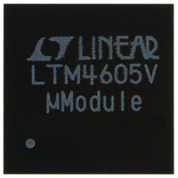
LTM4605IV#PBF Linear Technology, LTM4605IV#PBF Datasheet - Page 3

LTM4605IV#PBF
Manufacturer Part Number
LTM4605IV#PBF
Description
IC DC/DC UMODULE 5A 141-LGA
Manufacturer
Linear Technology
Series
µModuler
Type
Point of Load (POL) Non-Isolatedr
Datasheet
1.LTM4605EVPBF.pdf
(26 pages)
Specifications of LTM4605IV#PBF
Design Resources
LTM4605 Spice Model
Output
0.8 ~ 16 V
Number Of Outputs
1
Power (watts)
80W
Mounting Type
Surface Mount
Voltage - Input
4.5 ~ 20V
Package / Case
141-LGA
1st Output
0.8 ~ 16 VDC @ 5A
Size / Dimension
0.59" L x 0.59" W x 0.11" H (15mm x 15mm x 2.8mm)
Power (watts) - Rated
80W
Operating Temperature
-40°C ~ 85°C
Efficiency
98%
Dc To Dc Converter Type
Non-Inverting/Inverting/Step Up/Step Down
Pin Count
141
Input Voltage
20V
Output Voltage
0.8 to 16V
Switching Freq
170 TO 440KHz
Output Current
12/5A
Package Type
LGA
Output Type
Adjustable
Switching Regulator
Yes
Load Regulation
0.5%
Line Regulation
0.02%
Mounting
Surface Mount
Input Voltage (min)
4.5V
Operating Temperature Classification
Industrial
Lead Free Status / RoHS Status
Lead free / RoHS Compliant
3rd Output
-
2nd Output
-
Lead Free Status / Rohs Status
Compliant
Available stocks
Company
Part Number
Manufacturer
Quantity
Price
ELECTRICAL CHARACTERISTICS
temperature range, otherwise specifi cations are at T
SYMBOL
Output Specifi cations
I
ΔV
ΔV
Switch Section
M1 t
M1 t
M3 t
M3 t
M2, M4 t
M2, M4 t
t
t
t
t
Mode Transition 1
Mode Transition 2
M1 R
M2 R
M3 R
M4 R
Oscillator and Phase-Locked Loop
f
f
f
R
I
OUTDC
1d
2d
3d
4d
NOM
LOW
HIGH
PLLFLTR
PLLIN
FB
FB
r
f
r
f
/V
/V
DS(ON)
DS(ON)
DS(ON)
DS(ON)
FB(NOM)
FB(LOAD)
r
f
PARAMETER
Output Continuous Current Range
(See Output Current Derating Curves
for Different V
Reference Voltage Line Regulation
Accuracy
Load Regulation Accuracy
Turn-On Time (Note 4)
Turn-Off Time
Turn-On Time
Turn-Off Time
Turn-On Time
Turn-Off Time
M1 Off to M2 On Delay (Note 4)
M2 Off to M1 On Delay
M3 Off to M4 On Delay
M4 Off to M3 On Delay
M2 Off to M4 On Delay
M4 Off to M2 On Delay
Static Drain-to-Source On-Resistance
Static Drain-to-Source On-Resistance
Static Drain-to-Source On-Resistance
Static Drain-to-Source On-Resistance
Nominal Frequency
Lowest Frequency
Highest Frequency
PLLIN Input Resistance
Phase Detector Output Current
IN
, V
OUT
and T
A
)
A
= 25°C (Note 2), V
CONDITIONS
V
V
V
V
V
Drain to Source Voltage V
Bias Current I
Drain to Source Voltage V
Bias Current I
Drain to Source Voltage V
Bias Current I
Drain to Source Voltage V
Bias Current I
Drain to Source Voltage V
Bias Current I
Drain to Source Voltage V
Bias Current I
Drain to Source Voltage V
Bias Current I
Drain to Source Voltage V
Bias Current I
Drain to Source Voltage V
Bias Current I
Drain to Source Voltage V
Bias Current I
Drain to Source Voltage V
Bias Current I
Drain to Source Voltage V
Bias Current I
Bias Current I
Bias Current I
Bias Current I
Bias Current I
V
V
V
f
f
PLLIN
PLLIN
IN
IN
IN
COMP
COMP
PLLFLTR
PLLFLTR
PLLFLTR
= 12V, V
= 6V, V
= 4.5V to 20V, V
The
< f
> f
= 1.2V to 0.7V
= 1.2V to 1.8V (Note 3)
OSC
OSC
= 1.2V
= 0V
= 2.4V
l
OUT
denotes the specifi cations which apply over the full operating
OUT
SW
SW
SW
SW
SW
SW
SW
SW
SW
SW
SW
SW
SW
SW
SW
SW
= 12V
= 5V
= 10mA
= 10mA
= 10mA
= 10mA
= 10mA
= 10mA
= 10mA
= 10mA
= 10mA
= 10mA
= 10mA
= 10mA
= 3A
= 3A
= 3A
= 3A
COMP
IN
= 12V. Per typical application (front page) confi guration.
= 1.2V (Note 3)
DS
DS
DS
DS
DS
DS
DS
DS
DS
DS
DS
DS
= 12V,
= 12V,
= 12V,
= 12V,
= 12V,
= 12V,
= 12V,
= 12V,
= 12V,
= 12V,
= 12V,
= 12V,
l
l
MIN
260
170
340
–0.15
0.002
0.15
TYP
220
220
300
200
400
–15
6.5
12
50
40
25
20
20
20
50
50
50
50
50
15
5
8
8
8
LTM4605
MAX
0.02
–0.5
330
220
440
0.5
12
12
12
UNITS
4605fc
3
%/V
mΩ
mΩ
mΩ
mΩ
kHz
kHz
kHz
kΩ
μA
μA
ns
ns
ns
ns
ns
ns
ns
ns
ns
ns
ns
ns
%
%
A
A


