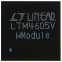
LTM4605IV#PBF Linear Technology, LTM4605IV#PBF Datasheet - Page 13

LTM4605IV#PBF
Manufacturer Part Number
LTM4605IV#PBF
Description
IC DC/DC UMODULE 5A 141-LGA
Manufacturer
Linear Technology
Series
µModuler
Type
Point of Load (POL) Non-Isolatedr
Datasheet
1.LTM4605EVPBF.pdf
(26 pages)
Specifications of LTM4605IV#PBF
Design Resources
LTM4605 Spice Model
Output
0.8 ~ 16 V
Number Of Outputs
1
Power (watts)
80W
Mounting Type
Surface Mount
Voltage - Input
4.5 ~ 20V
Package / Case
141-LGA
1st Output
0.8 ~ 16 VDC @ 5A
Size / Dimension
0.59" L x 0.59" W x 0.11" H (15mm x 15mm x 2.8mm)
Power (watts) - Rated
80W
Operating Temperature
-40°C ~ 85°C
Efficiency
98%
Dc To Dc Converter Type
Non-Inverting/Inverting/Step Up/Step Down
Pin Count
141
Input Voltage
20V
Output Voltage
0.8 to 16V
Switching Freq
170 TO 440KHz
Output Current
12/5A
Package Type
LGA
Output Type
Adjustable
Switching Regulator
Yes
Load Regulation
0.5%
Line Regulation
0.02%
Mounting
Surface Mount
Input Voltage (min)
4.5V
Operating Temperature Classification
Industrial
Lead Free Status / RoHS Status
Lead free / RoHS Compliant
3rd Output
-
2nd Output
-
Lead Free Status / Rohs Status
Compliant
Available stocks
Company
Part Number
Manufacturer
Quantity
Price
APPLICATIONS INFORMATION
output voltage falls by more than 70%, then the maximum
output current is progressively lowered to about 30% of
its full current limit value for boost mode and about 40%
for buck mode.
Standby Mode (STBYMD)
The standby mode (STBYMD) pin provides several choices
for start-up and standby operational modes. If the pin is
pulled to ground, the SS pin is internally pulled to ground,
preventing start-up and thereby providing a single control
pin for turning off the controller. If the pin is left open or
decoupled with a capacitor to ground, the SS pin is internally
provided with a starting current, permitting external control
for turning on the controller. If the pin is connected to a
voltage greater than 1.25V, the internal regulator (INTV
will be on even when the controller is shut down (RUN
pin voltage <1.6V). In this mode, the onboard 6V linear
regulator can provide power to keep-alive functions such
as a keyboard controller.
INTV
An internal P-channel low dropout regulator produces 6V
at the INTV
the control chip and internal circuitry within the module.
The LTM4605 also provides the external supply voltage pin
EXTV
5.7V, the internal regulator is turned off and an internal
switch connects the EXTV
supplying internal power. The switch remains closed as long
as the voltage applied to EXTV
allows the MOSFET driver and control power to be derived
from the output when (5.7V < V
internal regulator when the output is out of regulation (start-
up, short-circuit). If more current is required through the
EXTV
can be interposed between the EXTV
Ensure that EXTV
The following list summarizes the three possible connec-
tions for EXTV
1. EXTV
to be powered from the internal 6V regulator at the cost
of a small effi ciency penalty.
CC
CC
CC
. When the voltage applied to EXTV
and EXTV
CC
switch than is specifi ed, an external Schottky diode
left open (or grounded). This will cause INTV
CC
pin from the V
CC
:
CC
CC
≤ V
IN
CC
.
IN
pin to the INTV
CC
supply pin. INTV
remains above 5.5V. This
OUT
CC
< 7V) and from the
and INTV
CC
CC
rises above
pin thereby
CC
CC
powers
pins.
CC
CC
)
2. EXTV
3. EXTV
Thermal Considerations and Output Current Derating
In different applications, the LTM4605 operates in a variety
of thermal environments. The maximum output current is
limited by the environmental thermal condition. Suffi cient
cooling should be provided to ensure reliable operation.
When the cooling is limited, proper output current derating is
necessary, considering ambient temperature, airfl ow, input/
output condition, and the need for increased reliability.
The power loss curves in Figures 5 and 6 can be used
in coordination with the load current derating curves in
Figures 7 to 12 for calculating an approximate θ
the module. Column designation delineates between no
heat sink, and a BGA heat sink. Each of the load current
derating curves will lower the maximum load current as
a function of the increased ambient temperature to keep
the maximum junction temperature of the power module
at 115°C maximum. This will allow a safe margin to work
at the maximum operating temperature below 125°C.
Each of the derating curves and the power loss curve that
corresponds to the correct output voltage can be used to
solve for the approximate θ
explanation of the thermal characteristics is provided in
the thermal application note for the LTM4605.
DESIGN EXAMPLES
Buck Mode Operation
As a design example, use input voltage V
V
Set the PLLFLTR pin at 2.4V or more for 400kHz frequency
and connect FCB to ground for continuous current mode
operation. If a divider is used to set the frequency as shown
in Figure 14, the bottom resistor R3 is recommended not
to exceed 1k.
OUT
This is the normal connection for a 6V regulator and
provides the highest effi ciency.
supply is available in the 5.5V to 7V range, it may be
used to power EXTV
the MOSFET gate drive requirements.
= 12V and f = 400kHz.
CC
CC
connected directly to V
connected to an external supply. If an external
CC
provided it is compatible with
JA
of the condition. A complete
OUT
(5.7V < V
LTM4605
IN
= 12V to 20V,
OUT
13
< 7V).
JA
4605fc
for


