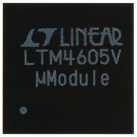
LTM4605IV#PBF Linear Technology, LTM4605IV#PBF Datasheet - Page 7

LTM4605IV#PBF
Manufacturer Part Number
LTM4605IV#PBF
Description
IC DC/DC UMODULE 5A 141-LGA
Manufacturer
Linear Technology
Series
µModuler
Type
Point of Load (POL) Non-Isolatedr
Datasheet
1.LTM4605EVPBF.pdf
(26 pages)
Specifications of LTM4605IV#PBF
Design Resources
LTM4605 Spice Model
Output
0.8 ~ 16 V
Number Of Outputs
1
Power (watts)
80W
Mounting Type
Surface Mount
Voltage - Input
4.5 ~ 20V
Package / Case
141-LGA
1st Output
0.8 ~ 16 VDC @ 5A
Size / Dimension
0.59" L x 0.59" W x 0.11" H (15mm x 15mm x 2.8mm)
Power (watts) - Rated
80W
Operating Temperature
-40°C ~ 85°C
Efficiency
98%
Dc To Dc Converter Type
Non-Inverting/Inverting/Step Up/Step Down
Pin Count
141
Input Voltage
20V
Output Voltage
0.8 to 16V
Switching Freq
170 TO 440KHz
Output Current
12/5A
Package Type
LGA
Output Type
Adjustable
Switching Regulator
Yes
Load Regulation
0.5%
Line Regulation
0.02%
Mounting
Surface Mount
Input Voltage (min)
4.5V
Operating Temperature Classification
Industrial
Lead Free Status / RoHS Status
Lead free / RoHS Compliant
3rd Output
-
2nd Output
-
Lead Free Status / Rohs Status
Compliant
Available stocks
Company
Part Number
Manufacturer
Quantity
Price
PIN FUNCTIONS
V
tween these pins and PGND pins. Recommend placing
input decoupling capacitance directly between V
and PGND pins.
V
between these pins and PGND pins. Recommend placing
output decoupling capacitance directly between these pins
and PGND pins.
PGND (Bank 6): Power Ground Pins for Both Input and
Output Returns.
SW1, SW2 (Bank 4, Bank 2): Switch Nodes. The power
inductor is connected between SW1 and SW2.
R
tor is connected from this pin to PGND.
SENSE
Reverse Current Detect Comparators.
SENSE
Reverse Current Detect Comparators.
EXTV
5.7V, an internal switch connects this pin to INTV
shuts down the internal regulator so that the controller and
gate drive power is drawn from EXTV
7V at this pin and ensure that EXTV
INTV
for additional decoupling of the 6V internal regulator.
PLLIN (Pin B9): External Clock Synchronization Input
to the Phase Detector. This pin is internally terminated
to SGND with a 50k resistor. The phase-locked loop will
force the rising bottom gate signal of the controller to be
synchronized with the rising edge of PLLIN signal.
PLLFLTR (Pin B8): The lowpass fi lter of the phase-locked
loop is tied to this pin. This pin can also be used to set the
frequency of the internal oscillator with an AC or DC voltage.
See the Applications Information section for details.
SS (Pin A6): Soft-Start Pin. Soft-start reduces the input
power sources’ surge currents by gradually increasing the
controller’s current limit.
IN
OUT
SENSE
(Bank 1): Power Input Pins. Apply input voltage be-
CC
CC
(Bank 5): Power Output Pins. Apply output load
+
–
(Bank 3): Sensing Resistor Pin. The sensing resis-
(Pin F5): Internal 6V Regulator Output. This pin is
(Pin F6): External V
(Pin A4): Positive Input to the Current Sense and
(Pin A5): Negative Input to the Current Sense and
CC
Input. When EXTV
CC
CC
< V
. Do not exceed
IN
.
CC
exceeds
IN
CC
pins
and
STBYMD (Pin A10): LDO Control Pin. Determine whether
the internal LDO remains active when the controller is shut
down. See Operations section for details. If the STBYMD
pin is pulled to ground, the SS pin is internally pulled to
ground to disable start-up and thereby providing a single
control pin for turning off the controller. An internal de-
coupling capacitor is tied to this pin.
V
Internally, this pin is connected to V
sion resistor. Different output voltages can be programmed
with an additional resistor between V
See the Applications Information section.
FCB (Pin A9): Forced Continuous Control Input. The
voltage applied to this pin sets the operating mode of the
module. When the applied voltage is less than 0.8V, the
forced continuous current mode is active. When this pin
is allowed to fl oat, the Burst Mode operation is active in
boost operation and the skip cycle mode is active in buck
operation. When the pin is tied to INTV
frequency discontinuous current mode is active in buck or
boost operation. See the Applications Information section.
SGND (Pin A7): Signal Ground Pin. This pin connects to
PGND at output capacitor point.
COMP (Pin B7): Current Control Threshold and Error
Amplifi er Compensation Point. The current comparator
threshold increases with this control voltage. The voltage
ranges from 0V to 2.4V.
PGOOD (Pin B5): Output Voltage Power Good Indicator.
Open drain logic output that is pulled to ground when
the output voltage is not within ±7.5% of the regulation
point.
RUN (Pin A8): Run Control Pin. A voltage below 1.6V will
turn off the module. There is a 100k resistor between the
RUN pin and SGND in the module. Do not apply more than
6V to this pin. See Applications Information section.
FB
(Pin B6): The Negative Input of the Error Amplifi er.
OUT
FB
LTM4605
with a 100k preci-
CC
and SGND pins.
, the constant
4605fc
7


