AD5247EVAL Analog Devices Inc, AD5247EVAL Datasheet - Page 14
AD5247EVAL
Manufacturer Part Number
AD5247EVAL
Description
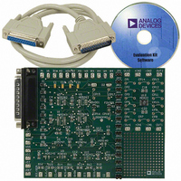
BOARD EVAL FOR AD5247
Manufacturer
Analog Devices Inc
Datasheet
1.AD5247BKSZ50-RL7.pdf
(20 pages)
Specifications of AD5247EVAL
Main Purpose
Digital Potentiometer
Utilized Ic / Part
AD5247
Lead Free Status / RoHS Status
Contains lead / RoHS non-compliant
Secondary Attributes
-
Embedded
-
Primary Attributes
-


AD5247
THEORY OF OPERATION
The AD5247 is a 128-position, digitally-controlled variable
resistor (VR) device. An internal power-on preset places the
wiper at midscale during power-on, which simplifies the
default condition recovery at power-up.
PROGRAMMING THE VARIABLE RESISTOR
Rheostat Operation
The nominal resistance (R
and Terminal B is available in 5 k Ω, 10 kΩ, 50 kΩ, and 100 kΩ. The
final two or three digits of the part number determine the nominal
resistance value; for example, 10 kΩ = 10 and 50 kΩ = 50. The
R
terminal, plus the B terminal contact. The 7-bit data in the
RDAC latch is decoded to select one of the 128 possible settings.
Assuming a 10 k Ω part is used, the wiper ’s first connection starts
at the B terminal for Data 0x00. Because there is a 50 Ω wiper
contact resistance, such a connection yields a minimum of 100 Ω
(2 × 50 Ω) resistance between Terminal W and Terminal B. The
second connection is the first tap point, corresponding to 178 Ω
(R
connection is the next tap point, representing 256 Ω (2 × 78 Ω
+ 2 × 50 Ω) for Data 0x02, and so on. Each LSB data value increase
moves the wiper up the resistor ladder until the last tap point is
reached at 10,100 Ω (R
Figure 35 shows a simplified diagram of the equivalent RDAC
circuit where the last resistor string is not accessed.
AB
WB
of the VR has 128 contact points accessed by the wiper
= R
AB
/128 + R
Figure 35. AD5247 Equivalent RDAC Circuit
D6
D5
D4
D3
D2
D1
D0
DECODER
LATCH
W
RDAC
AND
= 78 Ω + 2 × 50 Ω) for Data 0x01. The third
AB
+ 2 × R
R
R
R
AB
S
S
S
) of the RDAC between Terminal A
W
).
Ax
Wx
Bx
Rev. E | Page 14 of 20
The general equation determining the digitally programmed
output resistance between W and B is
where:
D is the decimal equivalent of the binary code loaded in the
7-bit RDAC register.
R
R
the internal switch.
In summary, if R
the output resistance R
RDAC latch codes.
Table 9. Codes and Corresponding R
D (Decimal)
127
64
1
0
Note that in the zero-scale condition, a finite resistance of
100 Ω between Terminal W and Terminal B is present. Care
should be taken to limit the current flow between W and B in
this state to a maximum pulse current of no more than 20 mA.
Otherwise, degradation or possible destruction of the internal
switch contact can occur.
Similar to the mechanical potentiometer, the resistance of
the RDAC between Wiper W and Terminal A also produces a
digitally controlled complementary resistance, R
these terminals are used, the Terminal B can be opened. Set the
resistance value for R
and to decrease the data loaded in the latch increases in value.
The general equation for this operation is
If R
resistance, R
latch codes.
Table 10. Codes and Corresponding R
D (Decimal)
127
64
1
0
Typical device-to-device matching is process lot dependent
and can vary by up to ±30%. Because the resistance element
is processed in thin film technology, the change in R
temperature has a very low 45 ppm/°C temperature coefficient.
AB
W
is the wiper resistance contributed by the on resistance of
AB
is the end-to-end resistance.
R
R
= 10 k Ω and the B terminal is open-circuited, the output
WB
WA
(D)
(D)
WA
=
=
, shown in Table 10, is set for the indicated RDAC
128
128
AB
D
R
10,072
5150
228
150
128
WB
= 10 k Ω and the Terminal A is open-circuited,
×
−
R
228
5150
10,071
10,150
(Ω)
WA
WA
R
D
WB
AB
to start at a maximum value of resistance
×
(Ω)
, shown in Table 9, is set for the indicated
R
+
AB
2
Output State
Full scale (R
Midscale
1 LSB
Zero scale (wiper contact resistance)
×
+
R
2
W
×
R
W
Output State
Full scale
Midscale
1 LSB
Zero scale
WB
AB
WA
+ 2 × R
Resistance
Resistance
W
WA
)
. When
AB
with
(1)
(2)
Related parts for AD5247EVAL
Image
Part Number
Description
Manufacturer
Datasheet
Request
R


Part Number:
Description:
±1.7g Dual-Axis IMEMS Accelerometer Evaluation Board
Manufacturer:
Analog Devices Inc
Datasheet:

Part Number:
Description:
Inertial Sensor Evaluation System
Manufacturer:
Analog Devices Inc
Datasheet:
Part Number:
Description:
Manufacturer:
Analog Devices Inc
Datasheet:
Part Number:
Description:
Manufacturer:
Analog Devices Inc
Datasheet:
Part Number:
Description:
Manufacturer:
Analog Devices Inc
Datasheet:
Part Number:
Description:
Manufacturer:
Analog Devices Inc
Datasheet:
Part Number:
Description:
Manufacturer:
Analog Devices Inc
Datasheet:
Part Number:
Description:
Manufacturer:
Analog Devices Inc
Datasheet:
Part Number:
Description:
Manufacturer:
Analog Devices Inc
Datasheet:
Part Number:
Description:
Manufacturer:
Analog Devices Inc
Datasheet:
Part Number:
Description:
Manufacturer:
Analog Devices Inc
Datasheet:
Part Number:
Description:
Manufacturer:
Analog Devices Inc
Datasheet: