AD5247EVAL Analog Devices Inc, AD5247EVAL Datasheet - Page 15
AD5247EVAL
Manufacturer Part Number
AD5247EVAL
Description
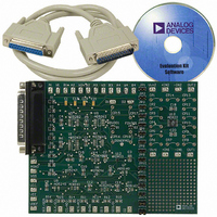
BOARD EVAL FOR AD5247
Manufacturer
Analog Devices Inc
Datasheet
1.AD5247BKSZ50-RL7.pdf
(20 pages)
Specifications of AD5247EVAL
Main Purpose
Digital Potentiometer
Utilized Ic / Part
AD5247
Lead Free Status / RoHS Status
Contains lead / RoHS non-compliant
Secondary Attributes
-
Embedded
-
Primary Attributes
-


PROGRAMMING THE POTENTIOMETER DIVIDER
Voltage Output Operation
The digital potentiometer easily generates a voltage divider at
wiper-to-B and wiper-to-A, proportional to the input voltage
at A-to-B. Unlike the polarity of V
positive, voltage across A-to-B, W-to-A, and W-to-B can be at
either polarity.
If ignoring the effect of the wiper resistance for approximation,
connecting the Terminal A to 5 V and the Terminal B to ground
produces an output voltage at the wiper-to-B starting at 0 V up
to 1 LSB less than 5 V. Each LSB of voltage is equal to the voltage
applied across Terminal A and Terminal B divided by the 128
positions of the potentiometer divider. The general equation
defining the output voltage at V
valid input voltage applied to Terminal A and Terminal B is
A more accurate calculation that includes the effect of wiper
resistance, V
Operation of the digital potentiometer in the divider mode
results in a more accurate operation over temperature. Unlike
rheostat mode, divider mode makes the output voltage mainly on
the ratio of Internal Resistor R
not the absolute values. Therefore, the temperature drift reduces
to 15 ppm/°C.
I
The first byte of the AD5247 is a slave address byte (see the I
Interface section). It has a 7-bit slave address and an R/ W bit.
The 5 kΩ and 50 kΩ options support one 7-bit slave address
while the 10 k Ω and 100 kΩ options each have three hard-coded
slave address options available (see Table 8 for a full list of slave
address locations). The extra hard coded slave addresses on the
10 kΩ and 100 kΩ options allow users to employ up to three of
these devices on one I
are followed by 0 for a write command or 1 to place the device
in read mode.
2
C-COMPATIBLE 2-WIRE SERIAL BUS
V
V
W
W
(D)
(
D
)
=
=
W
, is
R
128
D
WB
R
AB
(D)
×
V
2
C bus. The seven MSBs of the slave address
A
×
V
A
WA
W
to Internal Resistor R
with respect to ground for any
DD
to GND, which must be
WB
, and
2
Rev. E | Page 15 of 20
C
(3)
(4)
The 2-wire I
1.
2.
3.
4.
A repeated write function gives the user flexibility to update the
RDAC output a number of times after addressing the part only
once. For example, after the RDAC has acknowledged its slave
address in the write mode, the RDAC output updates on each
successive byte. If different instructions are needed, the write/read
mode has to start again with a new slave address and data byte.
Similarly, a repeated read function of the RDAC is also allowed.
The master initiates a data transfer by establishing a start
condition, which is when a high-to-low transition on the
SDA line occurs while SCL is high (see Figure 33). The
following byte is the slave address byte, consisting of the
7-bit slave address followed by an R/ W bit (this bit determines
whether data is read from or written to the slave device). The
slave, whose address corresponds to the transmitted address,
responds by pulling the SDA line low during the ninth clock
pulse (this is termed the acknowledge bit). At this stage, all
other devices on the bus remain idle while the selected
device waits for data to be written to or read from its serial
register. If the R/ W bit is high, the master reads from the
slave device. If the R/ W bit is low, the master writes to the
slave device.
In write mode, after acknowledgement of the slave address
byte, the next byte is the data byte. Data is transmitted over
the serial bus in sequences of nine clock pulses (eight data
bits followed by an acknowledge bit). The transitions on
the SDA line must occur during the low period of SCL
and remain stable during the high period of SCL (see
Figure 33).
In read mode, after acknowledgment of the slave address
byte, data is received over the serial bus in sequences of
nine clock pulses (a slight difference from write mode,
where eight data bits are followed by an acknowledge bit).
Similarly, the transitions on the SDA line must occur
during the low period of SCL and remain stable during
the high period of SCL (see Figure 34).
When all data bits have been read or written, a stop con-
dition is established by the master. A stop condition is
defined as a low-to-high transition on the SDA line while
SCL is high. In write mode, the master pulls the SDA line
high during the 10
(see Figure 33). In read mode, the master issues a no
acknowledge for the ninth clock pulse (that is, the SDA
line remains high). The master then brings the SDA line
low before the 10
a stop condition (see Figure 34).
2
C serial bus protocol operates as follows:
th
th
clock pulse, which goes high to establish
clock pulse to establish a stop condition
AD5247
Related parts for AD5247EVAL
Image
Part Number
Description
Manufacturer
Datasheet
Request
R


Part Number:
Description:
±1.7g Dual-Axis IMEMS Accelerometer Evaluation Board
Manufacturer:
Analog Devices Inc
Datasheet:

Part Number:
Description:
Inertial Sensor Evaluation System
Manufacturer:
Analog Devices Inc
Datasheet:
Part Number:
Description:
Manufacturer:
Analog Devices Inc
Datasheet:
Part Number:
Description:
Manufacturer:
Analog Devices Inc
Datasheet:
Part Number:
Description:
Manufacturer:
Analog Devices Inc
Datasheet:
Part Number:
Description:
Manufacturer:
Analog Devices Inc
Datasheet:
Part Number:
Description:
Manufacturer:
Analog Devices Inc
Datasheet:
Part Number:
Description:
Manufacturer:
Analog Devices Inc
Datasheet:
Part Number:
Description:
Manufacturer:
Analog Devices Inc
Datasheet:
Part Number:
Description:
Manufacturer:
Analog Devices Inc
Datasheet:
Part Number:
Description:
Manufacturer:
Analog Devices Inc
Datasheet:
Part Number:
Description:
Manufacturer:
Analog Devices Inc
Datasheet: