CDB48500-USB Cirrus Logic Inc, CDB48500-USB Datasheet
CDB48500-USB
Specifications of CDB48500-USB


Related parts for CDB48500-USB


CDB48500-USB Summary of contents
Page 1
... CDB48500-USB http://www.cirrus.com High-performance, 32-bit Audio Decoder DSP Family © Copyright 2008 Cirrus Logic, Inc. MAY 2008 DS784DB1 ...
Page 2
... CDB48500--USB Evaluation Kit Guide Contacting Cirrus Logic Support For all product questions and inquiries contact a Cirrus Logic Sales Representative. To find the one nearest to you MPORTANT NOTICE “Preliminary” product information describes products that are in production, but for which full characterization data is not yet available. ...
Page 3
... Contents Figures . . . . . . . . . . . . . . . . . . . . . . . . . . . . . . . . . . . . . . . . . . . . . . . . . . . . . . . . . . . . . . . . . . . . . . . 1-iv Tables .1-v Chapter 1. Introduction to the CRD48500-USB Evaluation Kit.......................... 1-1 1.1 CDB48500-USB Kit Contents and Requirements . . . . . . . . . . . . . . . . . . . . . . . . . . . . . . . . . .1-1 1.1.1 CDB48500-USB Kit ........................................................................................................1-1 1.1.2 PC Requirements ...........................................................................................................1-1 1.1.3 Software Requirements ..................................................................................................1-1 1.1.4 Support Hardware Requirements ...................................................................................1-1 1.1.5 Cabling Requirements ....................................................................................................1-1 1.2 Introducing the CDB48500-USB Customer Development Kit . . . . . . . . . . . . . . . . . . . . . . . .1-1 1 ...
Page 4
... A.1.1.1.11 Control Connector and Power ..................................................... A-4 Appendix B. Troubleshooting Guide ................................................................. B-1 B.1 Intoduction . . . . . . . . . . . . . . . . . . . . . . . . . . . . . . . . . . . . . . . . . . . . . . . . . . . . . . . . . . . . . . . . B-1 B.1.1 Solutions to Possible Problems..................................................................................... B-1 B.1.1.1 Power LEDs are Not illuminated .................................................................. B-1 B.1.1.2 CDB48500 is Not Recognized by the PC..................................................... B-1 B.1.1.3 Unable to Run a Stereo PCM Application .................................................... B-1 Revision History . . . . . . . . . . . . . . . . . . . . . . . . . . . . . . . . . . . . . . . . . . . . . . . . . . . . . . . . . . . . . . . B SPI)................................................................4-7 © ...
Page 5
... Figures Figure 1-1. CDB48500-USB System Block Diagram ......................................................................................... 1-2 Figure 1-2. CDB48500-USB Top View ............................................................................................................... 1-3 Figure 2-1. CDB USB MASTER Driver Setup .................................................................................................... 2-2 Figure 2-2. Board Setup Diagram ...................................................................................................................... 2-3 Figure 2-3. Found New Hardware Service Window ........................................................................................... 2-4 Figure 2-4. Found New Hardware Wizard Welcome Window ............................................................................ 2-4 Figure 2-5 ...
Page 6
... CDB48500--USB Evaluation Kit Guide vi © Copyright 2008 Cirrus Logic, Inc. DS784DB1 ...
Page 7
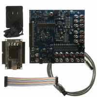
... Introducing the CDB48500-USB Customer Development Kit The CDB48500-USB kit is composed of the CDB48500 customer development board and the CDB USB MASTER Control board. The CDB48500 provides a practical platform for emulating a typical multi- channel audio system application. The CDB USB MASTER is a USB control board used to interface the ...
Page 8
... PC Figure 1-1. CDB48500-USB System Block Diagram This document will concentrate on the features and basic operation of the CDB48500-USB board. Detailed information regarding the operation and programming of the CS485XX DSP is covered by the CS485XX data sheet, CS485XX Hardware User’s Manual, and application note AN298 (see 1.2.2, “ ...
Page 9
... O.+1.8V Selection Header (Regulator/ External), J18 S.Analog Audio Outputs W.On-board/External Digital Audio Mux, U1 & U2 (U1 & U2 are on back of PCB.) Figure 1-2. CDB48500-USB Top View D.CS8416 S/PDIF Receiver, U3 H.Optical S/PDIF Input Jacks (PCM only), J2 L.Alternate +12V Jumper, J3 P.+1.8V Linear Regulator (1A), U14 T ...
Page 10
... The following information is located on the • CS8416 Data Sheet • CS8416 Errata 1. The “§§” symbol is used throughout this manual to indicate the end of the text flow in a chapter. DS784DB1 Introducing the CDB48500-USB Customer Development Kit www.cirrus.com Internet site: www.cirrus.com Internet site: 1 §§ ...
Page 11
... Introduction CDB48500-USB Evaluation Kit Guide Board Setup and Installing the Evaluation Kit Software 2.1 Introduction It is important to install the Evaluation Software BEFORE connecting the USB cable from the PC to the CDB USB MASTER card. Failure to install the evaluation software before the initial connection can result in an inability to communicate with the CBD485xx ...
Page 12
... Click Finish once the wizard has completed installation of the drivers. 12. The Cirrus DSP evaluation software will then prompt the user to click Finish to exit the Setup wizard. DS784DB1 Figure 2-1. CDB USB MASTER Driver Setup ©Copyright 2008 Cirrus Logic, Inc. Introduction CDB48500-USB Evaluation Kit Guide 2-2 ...
Page 13
... Introduction CDB48500-USB Evaluation Kit Guide 2.1.2 Setting up the Evaluation Kit Boards “B” USB Cable “A” USB 2.0 Port Power Cable 1. Place the CDB48500 and the CDB USB MASTER on a static-free surface the boards are not mated, connect them together as shown in connector on the CDB USB MASTER and the power connector on the CDB48500 are on the same side ...
Page 14
... Windows does not connect to Windows Update for the drivers. Click Next. Figure 2-4. Found New Hardware Wizard Welcome Window 5. Windows will then ask whether to use automatic installation or manual installation. Allow Windows to install the software automatically and click Next. DS784DB1 ©Copyright 2008 Cirrus Logic, Inc. Introduction CDB48500-USB Evaluation Kit Guide 2-4 ...
Page 15
... Introduction CDB48500-USB Evaluation Kit Guide Figure 2-5. Found New Hardware Wizard Finish Window possible that during the installation, Windows might issue a warning that the drivers have not passed “Windows Logo” testing. Select Continue Anyway. 7. Windows should now locate the correct drivers and complete the installation. ...
Page 16
... Neo6 , Audistry by Dolby local FAE to ensure the necessary licensing agreements have been completed. Please note that the CDB48500-USB does not support multi-channel decoding such as Dolby Digital CS485XX DSP is only a post-processor and does not contain a decoder. DS784DB1 → → Program Cirrus Logic DSP → ...
Page 17
... CDB485x00-USB Evaluation Kit Guide A detailed block diagram of the CDB48500 Customer Development Board is shown in sections that follow provide a detailed description of each block. Preamp Analog Analog Analog Analog Analog Analog In Inputs USB Clocks/Data SPI / I2C SPI FLASH I2C FLASH DAO Audio Out 3-1 ...
Page 18
... Connector Type: Fiber Optic RX for Digital Audio, JIS F05 (JIS C5974-1993 F05) • Reference Designator: J2, or SPDIF_RXP 3.1.1.3 Digital Coaxial Input Note: Digital Coaxial Input is PCM only as there is no multi-channel decoder present on CDB48500- USB. • Connector Type: RCA Female • Maximum Signal Level: +3.3V • ...
Page 19
... Connector Type: 1x3, 0.100 inch, Stake Header • Reference Designator: J17 - J19 The CDB48500-USB is designed to operate from a single DC power input. The 9V power supply provided with the kit is connected to the DC power input jack (J25) and is regulated down to the system voltages (5V, 3.3V, 1.8V). The power selection headers should be set to the ‘REG’ position when using the DC wall supply ...
Page 20
... CDB USB MASTER card The CS485XX has many applications stored in internal ROM, but a host is still required to configure the application for a particular system. The CDB48500-USB allows the PC to act as a host to boot and configure the DSP through the GUI software. The CS485XX can also be booted from external serial flash for custom applications that are not stored in the DSP’ ...
Page 21
... CS42448 Audio CODEC The CS42448 (U4 and U5 high-performance, multi-channel audio CODEC capable of supporting sample rates up to 192 kHz on its 6ADCs and 8 DACs. There are two of these devices on the CDB48500 and are used for all analog-to-digital and digital-to-analog conversions. All analog inputs (AIN_1A-AIN_6B) and all analog outputs (AOUT_1A-AOUT_6B) are connected to the CS42448s ...
Page 22
... MUXED_MCLK SDOUT DSP_SCLK SDIN DSP_LRCLK CS42448 DSP_DA0[3:0] CS42448 © Copyright 2008 Cirrus Logic , Inc. CDB48500 System Block Descriptions CDB485x00-USB Evaluation Kit Guide Use these jumper settings for the clocking mode and inputs shown in diagram. 8 Analog Inputs 2x 2x 4-3), and the audio ...
Page 23
... CDB48500 System Block Descriptions CDB485x00-USB Evaluation Kit Guide 3.1.11.2 Clock and Data Flow for S/PDIF Input CS8416 PLL DAO DAI CS485XX XMTA SPDIF OUT Figure 3-3. Simplified Clock and Data Flow for S/PDIF Input Figure 3-3 illustrates the S/PDIF clocking architecture used when any S/PDIF RX is used as an audio source, as described in Section 4.2.2, “ ...
Page 24
... LRCLK for the DAC side of the CS42448.The CS485XX always masters its output clocks (DSP_SCLK/ DSP_LRCLK). DS784DB1 MUXED_MCLK DSP_SCLK DSP_LRCLK DAO DSP_DA01[3:0] §§ © Copyright 2008 Cirrus Logic , Inc. CDB48500 System Block Descriptions CDB485x00-USB Evaluation Kit Guide SDIN CS42448 CS42448 2x 2x 4-3). MCLK is generated by the 3-8 ...
Page 25
... CS42448, the DAO port of the CS485XX and enables or disables the S/PDIF TX output port of the CS485XX. 4-1 Chapter 2, "Board Setup and Installing the Evaluation Kit Software" Section 2.1.4, “Running a Stereo PCM Application on CDB48500-USB” © Copyright 2008 Cirrus Logic , Inc. Chapter 4 Configuring the CDB48500 ...
Page 26
... Figure 4-1. PCM Pass-through Example Application 4.2.1 System Block The CDB48500 board is populated with a CS48560. However it is possible to evaluate the CS48520 and the CS48540 on this board. When you drag the system block on to the work space, a popup menu is displayed as shown in Figure When you select the target chip, place the template of the target chip on the analog connectors ...
Page 27
... Basic Application Download and System Configuration for PCM Pass-through CDB48500--USB Evaluation Kit Guide 4.2.2 Changing the Audio Input Source The audio input to the DSP is selected through the “Audio In” block in DSP Composer. The Audio can be delivered to the DSP via the following: • ...
Page 28
... SCLK Polarity • LRCLK Polarity • Temperature Grade - CDB48500s are populated with commercial-grade chips by default • Reference Clock - Set to the frequency of the crystal driving the CS485XX(Y1). This is the reference clock is used to determine the clock dividers needed to derive Fs in ADC-only applications. If this number changes, then all dividers for LRCLK/SCLK will change by the same ratio (e ...
Page 29
... CDB48500--USB Evaluation Kit Guide . 4.2.3 Changing Audio Output Configuration The audio output section of the CDB48500 is configured through the “Audio Out” block in DSP Composer. 4.2.3.1 DAO Output of CS485xx The digital audio output (DAO) of the CS485XX is very flexible, making it compatible with a wide variety of audio devices. This port can configured using the dialog box shown in “ ...
Page 30
... Figure 4-6. CDB48500 Digital Audio Output Properties This dialog allows the user to set the following parameters for the CS485XX Audio Output: • Mode - Master/slave settings for the SCLK & LRCLK pins. • Audio Data Format - I • SPDIF Enable - Checking this box configures DAO3 for S/PDIF output rather than I • ...
Page 31
... SCLK polarity - Slaves to the DAO Setting (Cannot be changed). 4.2.4 Changing Serial Control Protocol (I The CDB48500 is designed to communicate using either I communication mode in DSP Composer go to the menu bar and select File the Project Properties dialog. Click the Advanced button to get the Advanced Properties dialog as shown ...
Page 32
... Headphone Output The CDB48500 is designed with one Stereo Headphone output. The content of the Headphone output is controlled by the Remap tab in the SPP and APP module. The 2/HpL field is used to select the channel that will be output on the left channel and 3/HpR field is used to select the channel that will be output on the right channel ...
Page 33
... CDB48500--USB Evaluation Kit Guide 4.2.6 S/PDIF Transmitter The CDB48500 is designed with one S/PDIF Transmitter output. The content of the S/PDIF Transmitter output is controlled by the Remap tab in the SPP and APP module. The 6/SPDIF L is used to select the channel that will be output on the left channel and 7/SPDIF R is used to select the channel that will be output on the right channel ...
Page 34
... DS784DB1 Basic Application Download and System Configuration for PCM Pass-through © Copyright 2008 Cirrus Logic , Inc. CDB48500--USB Evaluation Kit Guide 4-10 ...
Page 35
... CDB48500--USB Evaluation Kit Guide A.1 Introduction Updates to the schematics for the CDB48500 Development Board can be can be obtained from your local Cirrus Logic representative as part of a design package including the associated BOM, and layout artwork. The schematics are provided in Adobe’s portable document format (PDF) and PADS™ format. ...
Page 36
... AOUT_4B. A.1.1.1.4 Serial Flash Memory (See The CDB48500 was designed with an Atmel 4 Mbit and SST 4 Mbit serial flash on-board. However only the SST Flash is connected to the DSP. To connect the Atmel part remove R101 and add a 0 Ohm resistor to R110. In addition to serial flash a 512 Kb Serial I devices and booting from them can be found in the AN298MPMF ...
Page 37
... Introduction CDB48500--USB Evaluation Kit Guide The CDB USB MASTER drives the serial host control port and CS8416_RESET signals on this page. The RCA jack for coaxial S/PDIF input and optical jack for optical S/PDIF input is listed on this page too. A.1.1.1.6 Codec #1(CS42448) (See The CS42448 is a multi-channel ADC/DAC that is capable of simultaneously supporting channels of analog input and 8 channels analog output ...
Page 38
... The DC input connector (J25) for the CDB48500 can accept capable of supplying at least 1 amp of current. The 3 voltage regulators on the CDB48500 generate the 1.8V, 3.3V, and 5V necessary for powering all of the ICs on the board. Note that the 5 V and 3.3 V regulators run directly off the DC input supply connected ...
Page 39
... Introduction CDB48500--USB Evaluation Kit Guide to the CDB48500, while the 1.8 V regulator is dependent upon 3.3 V system power (not necessarily the 3.3 V regulator). The 3 power jumpers (J17, J18, J19) are used to choose between the on-board regulators, and an external source for 5 V, 3.3 V, and 1.8 V. This is a feature intended only for special applications, so these jumpers should be left in the ‘ ...
Page 40
Figure A-1. CS48500 System Block Diagram ...
Page 41
Figure A-2. DSP Input Data Multiplexing ...
Page 42
Figure A-3. DSP ...
Page 43
Figure A-4. Serial Flash Memory ...
Page 44
Figure A-5. SPDIF Receiver ...
Page 45
Figure A-6. Codec #1(CS42448) ...
Page 46
Figure A-7. Codec #2 (CS42448) ...
Page 47
Figure A-8. Codec 1 and Codec 2 Input Filters ...
Page 48
Figure A-9. Output Filters & Headphone Output ...
Page 49
Figure A-10. Mic Preamp ...
Page 50
Figure A-11. Control Connector and Power §§ ...
Page 51
... Intoduction CDB48500--USB Evaluation Kit Guide B.1 Intoduction This chapter describes many common problems users may have with the CDB48500-USB, possible causes, and their solutions. B.1.1 Solutions to Possible Problems B.1.1.1 Power LEDs are Not illuminated • DC power supply is not connected to CDB48500 - make sure the DC wall supply is connected to the DC power input jack (J25), and the supply is plugged into a wall outlet. • ...
Page 52
... Revision History CDB48500--USB Evaluation Kit Guide B-2 §§ © Copyright 2008 Cirrus Logic , Inc. DS784DB1 ...