CDB48500-USB Cirrus Logic Inc, CDB48500-USB Datasheet - Page 37
CDB48500-USB
Manufacturer Part Number
CDB48500-USB
Description
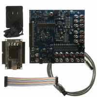
KIT USB EVALUATION FOR CDB48500
Manufacturer
Cirrus Logic Inc
Datasheet
1.CDB48500-USB.pdf
(52 pages)
Specifications of CDB48500-USB
Main Purpose
Audio, Audio Processing
Embedded
No
Utilized Ic / Part
CS485XX
Primary Attributes
32-Bit Audio Processor, I2C or SPI
Secondary Attributes
Graphic User Interface, 12-ch Analog Audio Input & Outputs, Optical Out- S/PDIF
Description/function
Audio A/D
Operating Supply Voltage
9 V to 12 V
Product
Audio Modules
Supply Current
1 A
For Use With/related Products
CS48520, CS48540, CS48560
Lead Free Status / RoHS Status
Contains lead / RoHS non-compliant
Lead Free Status / RoHS Status
Lead free / RoHS Compliant, Contains lead / RoHS non-compliant
Other names
598-1284


Introduction
CDB48500--USB Evaluation Kit Guide
A-3
The CDB USB MASTER drives the serial host control port and CS8416_RESET signals on this page.
The RCA jack for coaxial S/PDIF input and optical jack for optical S/PDIF input is listed on this page too.
The CS42448 is a multi-channel ADC/DAC that is capable of simultaneously supporting up to 6 channels
of analog input and 8 channels analog output. This is one of the two CODEC.
The serial host control port (SCL/CCLK, SDA/CDOUT, AD1/CDIN, AD0/CS) shares clock and data lines
with the CS485XX and CS8416. Both CODECS share the CS42448_CS line to this chip and driven only
when in SPI mode. The pull-ups required for the SCL and SDA pins are shared with the other devices on
the CDB48500 board.
The CS42448_RST signal is a dedicated reset signal driven by a general-purpose output of the CS8416.
The CS42448 is a slave to the MUXED_MCLK signal, which is the master audio clock for the entire
CDB48500 system.
The CS42448 masters the CS8416_SCLK and CS8416_LRCLK signals which are used to shift I
out of the CS42448 and shift I
The CS42448 slaves to the DSP_SCLK and DSP_LRCLK signals which are used to shift I
the CS485XX and shift I
The analog inputs and outputs of the CS42448 are being used in single-ended mode. This is evident
when looking at the input and output filter circuitry on page 6 of the schematics.
AIN5 of the CS42448 has an internal analog multiplexer that can be used to select between single-ended
inputs on the AIN5+ and AIN5- pins. This feature is used to share AIN5 between the microphone input
and RCA jack J5.
The transistor connected to MUTEC (Q1) provides the current drive necessary to drive all of the mute
transistors (see page 9 of schematic) into saturation.
The CDB USB MASTER drives the serial host control port signals on this page.
The CS42448 is a multi-channel ADC/DAC that is capable of simultaneously supporting up to 6 channels
of analog input and 8 channels analog output. This is one of the two CODEC.
The serial host control port (SCL/CCLK, SDA/CDOUT, AD1/CDIN, AD0/CS) shares clock and data lines
with the CS485XX and CS8416. Both CODECS share the CS42448_CS line to this chip and driven only
when in SPI mode. The pull-ups required for the SCL and SDA pins are shared with the other devices on
the CDB48500 board.
The CS42448_RST signal is a dedicated reset signal driven by a general-purpose output of the CS8416.
The CS42448 is a slave to the MUXED_MCLK signal, which is the master audio clock for the entire
CDB48500 system.
The CS42448 masters the CS8416_SCLK and CS8416_LRCLK signals which are used to shift I
out of the CS42448 and shift I
The CS42448 slaves to the DSP_SCLK and DSP_LRCLK signals which are used to shift I
the CS485XX and shift I
A.1.1.1.6 Codec #1(CS42448) (See
A.1.1.1.7 Codec #2 (CS42448) (See
2
2
S data into the CS42448.
S data into the CS42448.
2
2
S data into the CS485XX when ADC is used as the data input for the DSP.
S data into the CS485XX when ADC is used as the data input for the DSP.
©
Copyright 2008 Cirrus Logic , Inc.
Figure
Figure
A-6)
A-7)
2
2
S data out of
S data out of
DS784DB1
2
2
S data
S data
Related parts for CDB48500-USB
Image
Part Number
Description
Manufacturer
Datasheet
Request
R

Part Number:
Description:
Development Kit
Manufacturer:
Cirrus Logic Inc
Datasheet:
Part Number:
Description:
Development Kit
Manufacturer:
Cirrus Logic Inc
Datasheet:


Part Number:
Description:
High-efficiency PFC + Fluorescent Lamp Driver Reference Design
Manufacturer:
Cirrus Logic Inc
Datasheet:
Part Number:
Description:
Development Kit
Manufacturer:
Cirrus Logic Inc
Datasheet:
Part Number:
Description:
Development Kit
Manufacturer:
Cirrus Logic Inc
Datasheet:

Part Number:
Description:
Development Kit
Manufacturer:
Cirrus Logic Inc
Datasheet:
Part Number:
Description:
Development Kit
Manufacturer:
Cirrus Logic Inc
Datasheet:
Part Number:
Description:
Development Kit
Manufacturer:
Cirrus Logic Inc
Datasheet:
Part Number:
Description:
Development Kit
Manufacturer:
Cirrus Logic Inc
Datasheet:

Part Number:
Description:
EVALUATION BOARD FOR CS8427
Manufacturer:
Cirrus Logic Inc
Datasheet:

Part Number:
Description:
BOARD EVAL FOR CS8416 RCVR
Manufacturer:
Cirrus Logic Inc
Datasheet:

Part Number:
Description:
EVALUATION BOARD FOR CS8420
Manufacturer:
Cirrus Logic Inc
Datasheet:

Part Number:
Description:
KIT DEVELOPMENT EP9315 ARM9
Manufacturer:
Cirrus Logic Inc
Datasheet:

Part Number:
Description:
KIT DEVELOPMENT EP9302 ARM9
Manufacturer:
Cirrus Logic Inc
Datasheet: