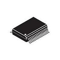
KIT33879AEKEVBE Freescale Semiconductor, KIT33879AEKEVBE Datasheet - Page 14

KIT33879AEKEVBE
Manufacturer Part Number
KIT33879AEKEVBE
Description
BOARD EVALUATION FOR MC33879
Manufacturer
Freescale Semiconductor
Type
PWM Controllersr
Specifications of KIT33879AEKEVBE
Main Purpose
Power Management, High & Low Side Driver (Internal FET)
Embedded
No
Utilized Ic / Part
MC33879
Primary Attributes
8-output hardware-configurable
Secondary Attributes
16-bit serial input control
Interface Type
SPI
Product
Power Management Modules
Silicon Manufacturer
Freescale
Silicon Core Number
MC33879
Kit Application Type
Power Management
Application Sub Type
Switch
Kit Contents
Board, CD
Rohs Compliant
Yes
Lead Free Status / RoHS Status
Lead free / RoHS Compliant
For Use With/related Products
MC33879
CS PIN
communicate through the use of the chip select
low on
data to be transferred from the MCU to the 33879 and vice
versa. Data clocked into the 33879 is acted upon on the rising
edge of
transition of the
is in a logic low state.
SCLK PIN
33879. The serial data input (DI) pin is latched into the input
shift register on the falling edge of the SCLK. The serial data
output (DO) pin shifts data out of the shift register on the
rising edge of the SCLK signal. False clocking of the shift
register must be avoided to ensure validity of data. It is
essential that the SCLK pin be in a logic low state when the
CS
recommended the SCLK pin is commanded to a logic low
state when the device is not accessed (
With
are ignored and the DO output is tri-state.
DI PIN
information is latched into the input register on the falling
edge of SCLK. A logic high state present on DI will program
a specific output on. The specific output will turn on with the
rising edge of the
present on the DI pin will program the output off. The specific
output will turn off with the rising edge of the
program the eight outputs and Open Load Detection Current
on or off, send the DI data beginning with the Open Load
Detection Current bits, followed by output eight, output
seven, and so on to output one. For each falling edge of the
SCLK while
loaded into the shift register per the data bit DI state. Sixteen
bits of entered information is required to fill the input shift
register.
DO PIN
remains tri-state until the
faults on the 33879 device are reported as logic [1] through
the DO data pin. Regardless of the configuration of the driver,
open loads and shorted loads are reported as logic [1].
Conversely, normal operating outputs with non-faulted loads
are reported as logic [0]. Outputs programmed with Open
Load Detection Current disabled will report logic [0] in the off
state. The first eight positive transitions of SCLK will report
14
33879
FUNCTIONAL DESCRIPTION
FUNCTIONAL PIN DESCRIPTION
The system MCU selects the 33879 with which to
To avoid any spurious data, it is essential the high-to-low
The SCLK pin clocks the internal shift registers of the
The DI pin is used for serial instruction data input. DI
The DO pin is the output from the shift register. The DO pin
pin makes any transition. For this reason, it is
CS
CS
CS
in a logic high state, signals present on SCLK and DI
enables the data output (DO) driver and allows
.
CS
is logic low, a data bit instruction (on or off) is
CS
CS
signal occur only when SPI clock (SCLK)
signal. Conversely, a logic low state
CS
pin is in a logic low state. All
CS
in logic high state).
FUNCTIONAL DESCRIPTION
FUNCTIONAL PIN DESCRIPTION
CS
CS
signal. To
pin. Logic
logic [0] followed by the status of the eight output drivers. The
DI / DO shifting of data follows a first-in, first-out protocol with
both input and output words transferring the most significant
bit (MSB) first.
EN PIN
pin high, output drivers may be activated and open / short fault
detection performed and reported. With the EN pin low, all
outputs become inactive, Open Load Detection Current is
disabled, and the device enters Sleep mode. The 33879 will
perform Power-ON Reset on rising edge of the enable signal.
IN5 AND IN6 PINS
six to be used in PWM applications. The IN5 and IN6 pins are
OR-ed with the Serial Peripheral Interface (SPI) command
input bits. For SPI control of outputs five and six, the IN5 and
IN6 pins should be grounded or held low by the
microprocessor. When using IN5 or IN6 to PWM the output,
the control SPI bit must be logic [0]. Maximum PWM
frequency for each output is 2.0 kHz.
VDD PIN
microprocessor interface (SPI) pins. Current from VDD is
used to drive DO output and the pullup current for
must be applied for normal mode operation. The 33879
device will perform Power-ON Reset with the application of
V
VPWR PIN
33879 IC. The VPWR pin has internal reverse battery
protection. All internal logic current is provided from the
VPWR pin. The 33879 will perform Power-ON Reset with the
application of V
D1– D8 PINS
For high side drive configurations, the drain pins are
connected to battery supply. In low side drive configurations,
the drain pins are connected to the low side of the load. All
outputs may be configured individually as desired. When
configured as low side drive, the 33879 limits the positive
inductive transient to 45 V.
S1– S8 PINS
high side drive configurations, the source pins are connected
directly to the load. In low side drive configurations, the
DD.
The EN pin on the 33879 enables the device. With the EN
The IN5 and IN6 command inputs allow outputs five and
The VDD input pin is used to determine logic levels on the
The V
The D1 to D8 pins are the open-drain outputs of the 33879.
The S1 to S8 pins are the source outputs of the 33879. For
PWR
pin is battery input and Power-ON Reset to the
PWR.
Analog Integrated Circuit Device Data
Freescale Semiconductor
CS
. V
DD


