LMX25313010EVAL National Semiconductor, LMX25313010EVAL Datasheet
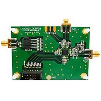
LMX25313010EVAL
Specifications of LMX25313010EVAL


Related parts for LMX25313010EVAL

LMX25313010EVAL Summary of contents
Page 1
... LMX2531LQ3010E Evaluation Board Operating Instructions National Semiconductor Corporation Timing Devices Business Group 10333 North Meridian Suite 400 Indianapolis, IN 46290 LMX25313010EVAL Instructions Rev 6.24.2009 ...
Page 2
Table of Contents Table of Contents ................................................................................................................ 2 Loop Filter .......................................................................................................................... 3 Quick Setup ......................................................................................................................... 3 Troubleshooting .................................................................................................................. 4 S OFTWARE DOES NOT COMMUNICATE WITH THE ...
Page 3
Loop Filter Loop Bandwidth 13.8 kHz Phase Margin 54.5 ° Crystal Frequency 10 MHz Supply Voltage 3.0 Volts Quick Setup • Install the CodeLoader software which ...
Page 4
Troubleshooting Software does not communicate with the evaluation boards LPT or USB Mode • Ensure a valid signal is presented to the OSCin connector ...
Page 5
Far-out Phase noise is worse than evaluation board instructions • Ensure the measurement equipment noise floor is not limiting the measurement. spectrum analyzers, the noise floor ...
Page 6
Phase Noise ...
Page 7
Free-Running VCO Phase Noise (Internal Divide by 2 Disabled ...
Page 8
Free-Running VCO Phase Noise (Internal Divide by 2 Enabled ...
Page 9
Fractional Spurs (Internal Divide by 2 Disabled ...
Page 10
Fractional Spurs (Internal Divide by 2 Enabled ...
Page 11
Integer Spurs (Internal Divide by 2 Disabled ...
Page 12
Integer Spurs (Internal Divide by 2 Enabled ...
Page 13
In-band Factional Spurs Integer Spurs (Internal Divide by 2 Disabled ...
Page 14
In-band Factional Spurs Integer Spurs (Internal Divide by 2 Enabled ...
Page 15
Inter-modulation Spurs The LMX2531 features an output divider which may divide the VCO frequency by two. The result is an Fout frequency half the VCO frequency. ...
Page 16
CodeLoader Settings CodeLoader runs many devices. necessary to select the correct device ...
Page 17
There can be different modes defined for a particular part. A mode can be recalled easily from the menu. This restores bit settings and frequencies, but ...
Page 18
The Bits/Pins tab displays many of the bits used to program the part. Right mouse click any bit to view more information about what this does. ...
Page 19
The PLL/VCO tab shows all the important PLL controls. Reference Oscillator should be programmed to the reference frequency connected to the OSCin of the evaluation board. ...
Page 20
The Registers tab shows the literal bits that are being sent to the part. These are the registers every time the PLL is loaded by using ...
Page 21
The port setup tells CodeLoader what information goes where. If this is wrong, the part will not program. Although LPT1 is usually correct, CodeLoader does NOT ...
Page 22
Schematic POWER 1 3 Vcc Vcc C1 R14 R16 R15 TRIGGER GND FRA ...
Page 23
Bill of Materials Bill of Materials Item QTY Manufacturer Part # ...
Page 24
Top Layer ...
Page 25
Mid Layer 1 "Ground Plane" ...
Page 26
Mid Layer 2 "Power" ...
Page 27
Bottom Layer "Signal" ...
Page 28
Top Build Diagram ...