ADP2114-2PH-EVALZ Analog Devices Inc, ADP2114-2PH-EVALZ Datasheet - Page 26
ADP2114-2PH-EVALZ
Manufacturer Part Number
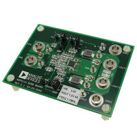
ADP2114-2PH-EVALZ
Description
BOARD EVALUATION 1.2V 4A 1.2MHZ
Manufacturer
Analog Devices Inc
Type
Evaluation Boardr
Specifications of ADP2114-2PH-EVALZ
Design Resources
Powering AD9268 with ADP2114 for Increased Efficiency (CN0137)
Main Purpose
DC/DC, Step Down
Outputs And Type
1, Non-Isolated
Voltage - Output
0.6 ~ 3.3 V
Current - Output
4A
Voltage - Input
2.75 ~ 5.5 V
Regulator Topology
Buck
Frequency - Switching
300kHz, 600kHz, 1.2MHz
Board Type
Fully Populated
Utilized Ic / Part
ADP2114
Svhc
No SVHC (18-Jun-2010)
Kit Features
DC-to-DC Switching Regulator, Standalone Capability, Configurable SYNC Input Or CLOCKOUT Output
Mcu Supported Families
ADP2114
Silicon Manufacturer
Analog Devices
Kit Contents
Board
Features
Standalone Capability, Two Independent Enable Inputs, Two Power Good Outputs
Core Architecture
Power
Rohs Compliant
Yes
Kit Application Type
Power Management
Application Sub Type
Step Down DC/DC Regulator
Lead Free Status / RoHS Status
Lead free / RoHS Compliant
Power - Output
-
Lead Free Status / RoHS Status
Lead free / RoHS Compliant, Lead free / RoHS Compliant
Available stocks
Company
Part Number
Manufacturer
Quantity
Price
Company:

Part Number:
ADP2114-2PH-EVALZ
Manufacturer:
Analog Devices Inc
Quantity:
135


ADP2114
OPERATION MODE CONFIGURATION
The dual-channel ADP2114 can be configured to one of the four
modes of operation by connecting the OPCFG pin as shown in
Table 7. This configuration sets the current limit for each
channel and enables or disables the transition to pulse skip mode
at light loads.
In the dual-phase configuration, the outputs of the two channels
are connected together, and they generate a single dc output
voltage, V
only Mode 2 in the OPCFG options can be used. In this mode,
the error amplifiers of both phases are used. The feedback
pins (FB1 and FB2) are tied together, the compensation pins
(COMP1 and COMP2) are tied together, the soft start pins (SS1
and SS2) are tied together, and the enable pins (EN1 and EN2)
are tied together.
Table 7. Current Limit Operation Mode and Configuration
Mode
1
2
3
4
OUT
R
0 to GND
4.7 k to GND
8.2 k to GND
15 k to GND
OPCFG
. For this single combined dual-phase output,
(Ω) ± 5%
Maximum Output Current
I
2/2
2/2
3/1
3/1
OUT1
(A)/I
OUT2
(A)
Rev. 0 | Page 26 of 40
Peak Current Limit
I
3.3/3.3
3.3/3.3
4.5/1.9
4.5/1.9
LIMIT1
In addition, if the power-good feature is used, combine PGOOD1
and PGOOD2 and connect them to VDD through a single
pull-up resistor.
When the ADP2114 is synchronized to an external clock, the
converters always operate in fixed frequency CCM, and they do
not enter into pulse skip mode at light loads. In this case, when
configuring the OPCFG pin, choose forced PWM mode.
(A)/I
LIMIT2
(A)
Power Savings at Light Load
Pulse skip enabled
Forced PWM
Pulse skip enabled
Forced PWM
Related parts for ADP2114-2PH-EVALZ
Image
Part Number
Description
Manufacturer
Datasheet
Request
R

Part Number:
Description:
BOARD EVALUATION 3.3V/1.8V
Manufacturer:
Analog Devices Inc
Datasheet:

Part Number:
Description:
Configurable, Dual 2 A/Single 4 A, Synchronous Step-Down DC-to-DC Regulator
Manufacturer:
Analog Devices
Datasheet:

Part Number:
Description:
Blank ADISimPower Eval ADP2114
Manufacturer:
Analog Devices Inc
Datasheet:

Part Number:
Description:
±1.7g Dual-Axis IMEMS Accelerometer Evaluation Board
Manufacturer:
Analog Devices Inc
Datasheet:
Part Number:
Description:
Inertial Sensor Evaluation System
Manufacturer:
Analog Devices Inc
Datasheet:
Part Number:
Description:
Manufacturer:
Analog Devices Inc
Datasheet:
Part Number:
Description:
Manufacturer:
Analog Devices Inc
Datasheet:
Part Number:
Description:
Manufacturer:
Analog Devices Inc
Datasheet:
Part Number:
Description:
Manufacturer:
Analog Devices Inc
Datasheet:
Part Number:
Description:
Manufacturer:
Analog Devices Inc
Datasheet:
Part Number:
Description:
Manufacturer:
Analog Devices Inc
Datasheet:
Part Number:
Description:
Manufacturer:
Analog Devices Inc
Datasheet:
Part Number:
Description:
Manufacturer:
Analog Devices Inc
Datasheet: