ADP2114-2PH-EVALZ Analog Devices Inc, ADP2114-2PH-EVALZ Datasheet - Page 30
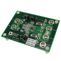
ADP2114-2PH-EVALZ
Manufacturer Part Number
ADP2114-2PH-EVALZ
Description
BOARD EVALUATION 1.2V 4A 1.2MHZ
Manufacturer
Analog Devices Inc
Type
Evaluation Boardr
Specifications of ADP2114-2PH-EVALZ
Design Resources
Powering AD9268 with ADP2114 for Increased Efficiency (CN0137)
Main Purpose
DC/DC, Step Down
Outputs And Type
1, Non-Isolated
Voltage - Output
0.6 ~ 3.3 V
Current - Output
4A
Voltage - Input
2.75 ~ 5.5 V
Regulator Topology
Buck
Frequency - Switching
300kHz, 600kHz, 1.2MHz
Board Type
Fully Populated
Utilized Ic / Part
ADP2114
Svhc
No SVHC (18-Jun-2010)
Kit Features
DC-to-DC Switching Regulator, Standalone Capability, Configurable SYNC Input Or CLOCKOUT Output
Mcu Supported Families
ADP2114
Silicon Manufacturer
Analog Devices
Kit Contents
Board
Features
Standalone Capability, Two Independent Enable Inputs, Two Power Good Outputs
Core Architecture
Power
Rohs Compliant
Yes
Kit Application Type
Power Management
Application Sub Type
Step Down DC/DC Regulator
Lead Free Status / RoHS Status
Lead free / RoHS Compliant
Power - Output
-
Lead Free Status / RoHS Status
Lead free / RoHS Compliant, Lead free / RoHS Compliant
Available stocks
Company
Part Number
Manufacturer
Quantity
Price
Company:

Part Number:
ADP2114-2PH-EVALZ
Manufacturer:
Analog Devices Inc
Quantity:
135


ADP2114
DESIGN EXAMPLE
The external component selection procedure from the Control
Loop Compensation section is used for this design example.
Table 9. 2-Channel Step-Down DC-to-DC Converter
Requirements
Parameter
Input Voltage, V
Channel 1, V
Channel 2, V
Pulse-Skip Feature
CHANNEL 1 CONFIGURATION AND COMPONENTS
SELECTION
Complete the following steps to configure Channel 1:
1.
2.
For the target output voltage, V
V1SET pin through a 47 kΩ resistor to GND (see Table 4).
Because one of the fixed output voltage options is chosen,
the feedback pin (FB1) must be directly connected to the
output of Channel 1, V
Estimate the duty-cycle, D, range. Ideally,
That gives the duty cycle for the 3.3 V output voltage and
the nominal input voltage of D
The minimum duty cycle, D
voltage (10% above the nominal) is D
maximum = 5.5 V
The maximum duty cycle, D
voltage (10% less than nominal) is D
minimum = 4.5 V.
However, the actual duty cycle is larger than the calculated
values to compensate for the power losses in the converter.
Therefore, add 5% to 7% at the maximum load.
Based on the estimated duty-cycle range, choose the
switching frequency according to the minimum and
maximum duty-cycle limitations, as shown in Figure 72.
For the Channel 1 V
choose f
This frequency option provides the smallest sized solution.
If a higher efficiency is required, choose the 300 kHz option.
However, the PCB footprint area of the converter will be
larger because of the bigger inductor and output capacitors.
D =
V
V
OUT
IN
OUT1
OUT2
SW
IN
= 600 kHz with a maximum duty cycle of 0.8.
Specification
5.0 V ±10%
3.3 V, 2 A, 1% V
ripple (p-p)
1.8 V, 2 A, 1% V
ripple (p-p)
Enabled
IN
= 5 V and V
OUT1
.
MIN
MAX
NOM
, for the maximum input
OUT
OUT
OUT
, for the minimum input
OUT
= 0.66 at V
= 3.3 V, connect the
= 3.3 V combination,
MAX
MIN
Additional
Requirements
None
Maximum load step:
1 A to 2 A, 5% droop
maximum
Maximum load step:
1 A to 2 A, 5% droop
maximum
None
= 0.73 at V
= 0.60 at V
IN
= 5.0 V.
IN
IN
(20)
Rev. 0 | Page 30 of 40
3.
4.
5.
Select the inductor by using Equation 5.
In Equation 5, V
and f
Therefore, when L = 3.3 μH (the closest standard value) in
Equation 3, ΔI
Although the maximum output current required is 2 A, the
maximum peak current is 3.3 A under the current limit
condition (see Table 7). Therefore, the inductor should be
rated for 3.3 A of peak current and 3 A of average current
for reliable circuit operation.
Select the output capacitor by using Equation 8 and
Equation 9.
Equation 8 is based on the output ripple (ΔV
Equation 9 is for capacitor selection based on the transient
load performance requirements that allow, in this case, 5%
maximum deviation. As previously mentioned, perform
these calculations and choose whatever equation yields the
larger capacitor size.
In this case, the following values are substituted for the
variables in Equation 8 and Equation 9:
ΔI
f
ΔV
ESR = 3 mΩ (typical for ceramic capacitors)
ΔI
ΔV
The output ripple based calculation (see Equation 8) dictates
that C
calculation (see Equation 9) dictates that C
meet both requirements, choose the latter. As previously
mentioned in the Control Loop Compensation section, the
capacitor value reduces with applied dc bias; therefore, select a
higher value. In this case, the next higher value is 47 μF
with a minimum voltage rating of 6.3 V.
Calculate the feedback loop, compensation component
values by using Equation 15.
H(s) = g
L
C
C
SW
OUT_MIN
OUT_MIN
=
L
OUT_STEP
= 600 kHz
RIPPLE
DROOP
= 0.566 A
(
SW
V
Δ
OUT
IN
= 600 kHz, which results in L = 3.11 μH.
I
M
L
= 33 mV (1% of 3.3 V)
= 0.165 V (5% of 3.3 V)
≅
= 4.0 μF, whereas the transient load based
−
× G
×
≅
= 1 A
V
8
ΔI
f
OUT
×
SW
CS
OUT_STEP
L
f
SW
IN
×
= 0.566 A.
)
×
= 5 V, V
×
V
V
V
(
V
OUT
REF
ΔV
OUT
IN
×
RIPPLE
ΔI
⎛
⎜
⎜
⎝
× Z
OUT
f
L
SW
COMP
-
= 3.3 V, ΔI
ΔI
×
ΔV
L
3
(s) × Z
×
DROOP
ESR
L
)
FILT
= 0.3 × I
⎞
⎟
⎟
⎠
OUT
(s)
RIPPLE
= 30 μF. To
L
= 0.6 A,
), and
Related parts for ADP2114-2PH-EVALZ
Image
Part Number
Description
Manufacturer
Datasheet
Request
R

Part Number:
Description:
BOARD EVALUATION 3.3V/1.8V
Manufacturer:
Analog Devices Inc
Datasheet:

Part Number:
Description:
Configurable, Dual 2 A/Single 4 A, Synchronous Step-Down DC-to-DC Regulator
Manufacturer:
Analog Devices
Datasheet:

Part Number:
Description:
Blank ADISimPower Eval ADP2114
Manufacturer:
Analog Devices Inc
Datasheet:

Part Number:
Description:
±1.7g Dual-Axis IMEMS Accelerometer Evaluation Board
Manufacturer:
Analog Devices Inc
Datasheet:
Part Number:
Description:
Inertial Sensor Evaluation System
Manufacturer:
Analog Devices Inc
Datasheet:
Part Number:
Description:
Manufacturer:
Analog Devices Inc
Datasheet:
Part Number:
Description:
Manufacturer:
Analog Devices Inc
Datasheet:
Part Number:
Description:
Manufacturer:
Analog Devices Inc
Datasheet:
Part Number:
Description:
Manufacturer:
Analog Devices Inc
Datasheet:
Part Number:
Description:
Manufacturer:
Analog Devices Inc
Datasheet:
Part Number:
Description:
Manufacturer:
Analog Devices Inc
Datasheet:
Part Number:
Description:
Manufacturer:
Analog Devices Inc
Datasheet:
Part Number:
Description:
Manufacturer:
Analog Devices Inc
Datasheet: