DK86065-2 Fujitsu Semiconductor America Inc, DK86065-2 Datasheet - Page 21
DK86065-2
Manufacturer Part Number
DK86065-2
Description
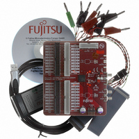
KIT EVAL 16BIT DAC FOR MB86065
Manufacturer
Fujitsu Semiconductor America Inc
Specifications of DK86065-2
Number Of Dac's
1
Number Of Bits
14
Outputs And Type
1, Differential
Sampling Rate (per Second)
1G
Data Interface
Serial
Dac Type
Current
Voltage Supply Source
Analog and Digital
Operating Temperature
-40°C ~ 85°C
Utilized Ic / Part
MB86065
For Use With
865-1111 - DAC DK FPGA ADAPTER BOARD865-1012 - KIT DEV DUAL 14BIT MB86064 SMA
Lead Free Status / RoHS Status
Lead free / RoHS Compliant
Other names
865-1011


September 2007 Version 1.01
FME/MS/DAC80S/DS/5344
MB86065 14-bit 1+GSa/s DAC
3
Enabling the Waveform Memory Module allows interleaving of LVDS data from both ports to drive
the DAC core as well as access to any downloaded waveforms. The on-chip waveform memories
allow the DAC core to be exercised with user programmable waveforms without the need for an
external high speed pattern generator. The memories are physically implemented using four 2k x 64-
bit static RAMs, assigned as two banks of ODD and EVEN samples. The memories can be
configured to hold two different waveforms of equal length, up to 16k points each, to be routed to the
DAC core as required. Alternatively, it is possible to download multiple waveforms, totalling 16k
points or less, to be selected as required. This last configuration takes advantage of the ability to
specify the waveform start address and length.
Data routing within the Waveform Memory Module is determined by three cascaded multiplexers,
mux_a_ctrl[0:2], as illustrated in Figure 13.
Copyright © 2004-2007 Fujitsu Microelectronics Europe GmbH
Disclaimer : The contents of this document are subject to change without notice. Customers are advised to consult with FUJITSU sales representatives before
Port A data input
Port B data input
14-bit LVDS
14-bit LVDS
Waveform Memory Module
ordering.The information and circuit diagrams in this document are presented “as is”, no license is granted by implication or otherwise.
The DAC exhibits a pipeline delay through the device of ~28 input clock edges when LVDS
data is routed via the WMM. The exact number of edges depends on the mode selected.
Waveform
Waveform
(Even & Odd)
(Even & Odd)
16K x 16-bit
16K x 16-bit
Waveform
Memory
Waveform
Memory
(Even & Odd)
(Even & Odd)
16K x 16-bit
16K x 16-bit
Memory
Memory
A
B
mux_a_ctrl[3:2]
A
B
Figure 13 Waveform Memory Module Data Routing
mux_a_ctrl[1]
en_int_term
0x1C4 - pg12
en_int_term
0x1C4 - pg11
mux_a_ctrl[0]
Production
data_direct
0x00 - pg13
DAC
(14-bit)
Page 21 of 56
Related parts for DK86065-2
Image
Part Number
Description
Manufacturer
Datasheet
Request
R

Part Number:
Description:
IC POWER SUPPLY MONITOR 8SOP
Manufacturer:
Fujitsu Semiconductor America Inc
Datasheet:
Part Number:
Description:
IC POWER SUPPLY MONITOR 8SOP
Manufacturer:
Fujitsu Semiconductor America Inc
Datasheet:

Part Number:
Description:
IC MCU 60K FLASH 2KB RAM 52LQFP
Manufacturer:
Fujitsu Semiconductor America Inc
Datasheet:

Part Number:
Description:
IC MCU 32BIT 256KB FLASH 120LQFP
Manufacturer:
Fujitsu Semiconductor America Inc
Datasheet:
Part Number:
Description:
IC CTLR TOUCH SENSOR 12CH 30SSOP
Manufacturer:
Fujitsu Semiconductor America Inc
Datasheet:

Part Number:
Description:
IC CTLR TOUCH SENSOR 12CH 40QFN
Manufacturer:
Fujitsu Semiconductor America Inc
Datasheet:
Part Number:
Description:
SYNTHESIZER PLL DUAL INP 20SSOP
Manufacturer:
Fujitsu Semiconductor America Inc
Datasheet:

Part Number:
Description:
SYNTHESZR PLL 1.1GHZ DUAL 16SSOP
Manufacturer:
Fujitsu Semiconductor America Inc
Datasheet:

Part Number:
Description:
IC SSCG EMI RED 8-SOIC
Manufacturer:
Fujitsu Semiconductor America Inc
Datasheet:

Part Number:
Description:
IC SSCG EMI RED 8-TSSOP
Manufacturer:
Fujitsu Semiconductor America Inc
Datasheet:

Part Number:
Description:
IC SSCG EMI RED 8-SOP
Manufacturer:
Fujitsu Semiconductor America Inc
Datasheet:

Part Number:
Description:
SYNTHESIZER PLL 2.5GHZ 16SSOP
Manufacturer:
Fujitsu Semiconductor America Inc
Datasheet:
Part Number:
Description:
SYNTHESIZER PLL 1.2GHZ 16SSOP
Manufacturer:
Fujitsu Semiconductor America Inc
Datasheet:

Part Number:
Description:
SYNTHESIZER PLL 2.5GHZ 16BCC
Manufacturer:
Fujitsu Semiconductor America Inc
Datasheet:

Part Number:
Description:
IC SSCG EMI RED 8-SOP
Manufacturer:
Fujitsu Semiconductor America Inc
Datasheet: