DK86065-2 Fujitsu Semiconductor America Inc, DK86065-2 Datasheet - Page 41
DK86065-2
Manufacturer Part Number
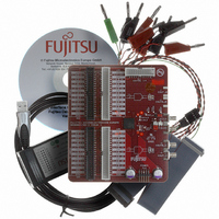
DK86065-2
Description
KIT EVAL 16BIT DAC FOR MB86065
Manufacturer
Fujitsu Semiconductor America Inc
Specifications of DK86065-2
Number Of Dac's
1
Number Of Bits
14
Outputs And Type
1, Differential
Sampling Rate (per Second)
1G
Data Interface
Serial
Dac Type
Current
Voltage Supply Source
Analog and Digital
Operating Temperature
-40°C ~ 85°C
Utilized Ic / Part
MB86065
For Use With
865-1111 - DAC DK FPGA ADAPTER BOARD865-1012 - KIT DEV DUAL 14BIT MB86064 SMA
Lead Free Status / RoHS Status
Lead free / RoHS Compliant
Other names
865-1011


September 2007 Version 1.01
FME/MS/DAC80S/DS/5344
MB86065 14-bit 1+GSa/s DAC
6
6.1
The following guidelines are suggestions to help obtain best performance from the MB86065. The
information may be subject to change.
The ground plane should not be split into the digital and analog regions. The digital and analog power
planes must be split as these are different voltages.
All supplies should be decoupled using surface mount 100nF to 1µF capacitors, placed as close as
possible to the device. For each pair of DVDD/DVSS pins it is recommended that the capacitor is
located on the reverse of the PCB, immediately under the device, with vias to the supply and ground
planes as close as possible to the device and capacitor. This layout minimizes tracking, including the
plated through hole, and hence keeps loop inductance to a minimum. See Figure 19 (0603 size
capacitors used).
For the analog supplies, the decoupling scheme in Figure 19 should be used. This scheme uses
seven 0603 100nF capacitors. This allows the decoupling capacitors, that also need to be placed
close to the device, to be fitted into a small area.
Deviation from the layout in Figure 19 is not recommended as the device pinout has been carefully
developed alongside this PCB design to give optimum performance. For single component-sided
PCB designs all decoupling capacitors should be placed in a ring around the edge of the device as
close as the assembly process will allow. The position of the capacitors should be such as to
minimise the distance from the ball, and the tracking must run directly from the supply ball to the
capacitor. Positioning the decouplers close to the device is the highest priority layout consideration.
Of the analog decouplers, the VREF to AVSS 100nF capacitor has the lowest priority (so is not shown
in Figure 19), however this decoupler should be positioned as close as reasonably practical to the
device.
The central array of thermal/ground balls should be connected directly to the ground plane. This array
has two functions. Firstly it connects the substrate to the ground plane that is most able to collect the
noise from the mostly digital regions of the die. Secondly, the thermal array is used to conduct heat
directly out of the die and into the PCB ground plane for heat spreading. The design of the PCB
around the thermal/ground array is critical for maximum heat transfer and ground plane integrity.
Copyright © 2004-2007 Fujitsu Microelectronics Europe GmbH
Disclaimer : The contents of this document are subject to change without notice. Customers are advised to consult with FUJITSU sales representatives before
Application Notes
PCB Power & Ground Plane Splits and Decoupling
ordering.The information and circuit diagrams in this document are presented “as is”, no license is granted by implication or otherwise.
Even though a common ground plane is recommended, ‘analog’ and ‘digital’ grounds
should not be linked on the top surface of the PCB even where this may appear convenient
to do so. Use separate vias to connect directly to the common ground plane.
Tracking and vias should be excluded from the zone highlighted in Figure 19(a). This
recommendation is to maximise separation between LVDS data bits in proximity of the
analog outputs.
A Fujitsu Design Guide, ‘PCB Design Rules for EFBGA Packages’, document number
FME/MS/APPS/DG/4568, provides a detailed description of the recommended PCB
design principles for this package.
Production
Page 41 of 56
Related parts for DK86065-2
Image
Part Number
Description
Manufacturer
Datasheet
Request
R

Part Number:
Description:
IC POWER SUPPLY MONITOR 8SOP
Manufacturer:
Fujitsu Semiconductor America Inc
Datasheet:
Part Number:
Description:
IC POWER SUPPLY MONITOR 8SOP
Manufacturer:
Fujitsu Semiconductor America Inc
Datasheet:

Part Number:
Description:
IC MCU 60K FLASH 2KB RAM 52LQFP
Manufacturer:
Fujitsu Semiconductor America Inc
Datasheet:

Part Number:
Description:
IC MCU 32BIT 256KB FLASH 120LQFP
Manufacturer:
Fujitsu Semiconductor America Inc
Datasheet:
Part Number:
Description:
IC CTLR TOUCH SENSOR 12CH 30SSOP
Manufacturer:
Fujitsu Semiconductor America Inc
Datasheet:

Part Number:
Description:
IC CTLR TOUCH SENSOR 12CH 40QFN
Manufacturer:
Fujitsu Semiconductor America Inc
Datasheet:
Part Number:
Description:
SYNTHESIZER PLL DUAL INP 20SSOP
Manufacturer:
Fujitsu Semiconductor America Inc
Datasheet:

Part Number:
Description:
SYNTHESZR PLL 1.1GHZ DUAL 16SSOP
Manufacturer:
Fujitsu Semiconductor America Inc
Datasheet:

Part Number:
Description:
IC SSCG EMI RED 8-SOIC
Manufacturer:
Fujitsu Semiconductor America Inc
Datasheet:

Part Number:
Description:
IC SSCG EMI RED 8-TSSOP
Manufacturer:
Fujitsu Semiconductor America Inc
Datasheet:

Part Number:
Description:
IC SSCG EMI RED 8-SOP
Manufacturer:
Fujitsu Semiconductor America Inc
Datasheet:

Part Number:
Description:
SYNTHESIZER PLL 2.5GHZ 16SSOP
Manufacturer:
Fujitsu Semiconductor America Inc
Datasheet:
Part Number:
Description:
SYNTHESIZER PLL 1.2GHZ 16SSOP
Manufacturer:
Fujitsu Semiconductor America Inc
Datasheet:

Part Number:
Description:
SYNTHESIZER PLL 2.5GHZ 16BCC
Manufacturer:
Fujitsu Semiconductor America Inc
Datasheet:

Part Number:
Description:
IC SSCG EMI RED 8-SOP
Manufacturer:
Fujitsu Semiconductor America Inc
Datasheet: