DEMO9S08DZ60 Freescale Semiconductor, DEMO9S08DZ60 Datasheet - Page 13
DEMO9S08DZ60
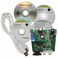
Manufacturer Part Number
DEMO9S08DZ60
Description
BOARD DEMO
Manufacturer
Freescale Semiconductor
Type
MCUr
Datasheets
1.DEMO9S08DZ60.pdf
(416 pages)
2.DEMO9S08DZ60.pdf
(1 pages)
3.DEMO9S08DZ60.pdf
(16 pages)
4.DEMO9S08DZ60.pdf
(2 pages)
5.DEMO9S08DZ60.pdf
(1 pages)
Specifications of DEMO9S08DZ60
Contents
Board, Cable, CD
Processor To Be Evaluated
MC9S08DZ60
Interface Type
RS-232, USB
Silicon Manufacturer
Freescale
Core Architecture
HCS08
Core Sub-architecture
HCS08
Silicon Core Number
MC9S08
Silicon Family Name
S08D
Kit Contents
MC9S08DZ60 Board, Software, Cables, Connectors
Rohs Compliant
Yes
For Use With/related Products
MC9S08DZ60
Lead Free Status / RoHS Status
Lead free / RoHS Compliant


Section Number
10.2 External Signal Description ...........................................................................................................178
10.3 Register Definition .........................................................................................................................179
10.4 Functional Description ...................................................................................................................187
10.5 Initialization Information ...............................................................................................................193
10.6 Application Information.................................................................................................................195
11.1 Introduction ....................................................................................................................................199
11.2 External Signal Description ...........................................................................................................202
Freescale Semiconductor
10.1.7 ADC Module Block Diagram .........................................................................................177
10.2.1 Analog Power (V
10.2.2 Analog Ground (V
10.2.3 Voltage Reference High (V
10.2.4 Voltage Reference Low (V
10.2.5 Analog Channel Inputs (ADx) ........................................................................................179
10.3.1 Status and Control Register 1 (ADCSC1) ......................................................................179
10.3.2 Status and Control Register 2 (ADCSC2) ......................................................................181
10.3.3 Data Result High Register (ADCRH) .............................................................................181
10.3.4 Data Result Low Register (ADCRL) ..............................................................................182
10.3.5 Compare Value High Register (ADCCVH) ....................................................................182
10.3.6 Compare Value Low Register (ADCCVL) .....................................................................183
10.3.7 Configuration Register (ADCCFG) ................................................................................183
10.3.8 Pin Control 1 Register (APCTL1) ..................................................................................184
10.3.9 Pin Control 2 Register (APCTL2) ..................................................................................185
10.3.10Pin Control 3 Register (APCTL3) ..................................................................................186
10.4.1 Clock Select and Divide Control ....................................................................................188
10.4.2 Input Select and Pin Control ...........................................................................................188
10.4.3 Hardware Trigger ............................................................................................................188
10.4.4 Conversion Control .........................................................................................................188
10.4.5 Automatic Compare Function .........................................................................................191
10.4.6 MCU Wait Mode Operation ............................................................................................191
10.4.7 MCU Stop3 Mode Operation ..........................................................................................192
10.4.8 MCU Stop2 Mode Operation ..........................................................................................192
10.5.1 ADC Module Initialization Example .............................................................................193
10.6.1 External Pins and Routing ..............................................................................................195
10.6.2 Sources of Error ..............................................................................................................196
11.1.1 Features ...........................................................................................................................201
11.1.2 Modes of Operation ........................................................................................................201
11.1.3 Block Diagram ................................................................................................................202
11.2.1 SCL — Serial Clock Line ...............................................................................................202
11.2.2 SDA — Serial Data Line ................................................................................................202
Inter-Integrated Circuit (S08IICV2)
DDAD
SSAD
MC9S08DZ60 Series Data Sheet, Rev. 4
) ..................................................................................................179
) .................................................................................................179
REFL
REFH
Chapter 11
) .....................................................................................179
) ...................................................................................179
Title
Page
13
Related parts for DEMO9S08DZ60
Image
Part Number
Description
Manufacturer
Datasheet
Request
R

Part Number:
Description:
Manufacturer:
Freescale Semiconductor, Inc
Datasheet:
Part Number:
Description:
Manufacturer:
Freescale Semiconductor, Inc
Datasheet:
Part Number:
Description:
Manufacturer:
Freescale Semiconductor, Inc
Datasheet:
Part Number:
Description:
Manufacturer:
Freescale Semiconductor, Inc
Datasheet:
Part Number:
Description:
Manufacturer:
Freescale Semiconductor, Inc
Datasheet:
Part Number:
Description:
Manufacturer:
Freescale Semiconductor, Inc
Datasheet:
Part Number:
Description:
Manufacturer:
Freescale Semiconductor, Inc
Datasheet:
Part Number:
Description:
Manufacturer:
Freescale Semiconductor, Inc
Datasheet:
Part Number:
Description:
Manufacturer:
Freescale Semiconductor, Inc
Datasheet:
Part Number:
Description:
Manufacturer:
Freescale Semiconductor, Inc
Datasheet:
Part Number:
Description:
Manufacturer:
Freescale Semiconductor, Inc
Datasheet:
Part Number:
Description:
Manufacturer:
Freescale Semiconductor, Inc
Datasheet:
Part Number:
Description:
Manufacturer:
Freescale Semiconductor, Inc
Datasheet:
Part Number:
Description:
Manufacturer:
Freescale Semiconductor, Inc
Datasheet:
Part Number:
Description:
Manufacturer:
Freescale Semiconductor, Inc
Datasheet: