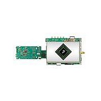
MCIMX35WPDKJ Freescale Semiconductor, MCIMX35WPDKJ Datasheet - Page 145

MCIMX35WPDKJ
Manufacturer Part Number
MCIMX35WPDKJ
Description
BOARD DEV FOR I.MX35
Manufacturer
Freescale Semiconductor
Series
i.MX35r
Type
MPUr
Datasheets
1.MCIMX35WPDKJ.pdf
(148 pages)
2.MCIMX35WPDKJ.pdf
(2 pages)
3.MCIMX35WPDKJ.pdf
(10 pages)
Specifications of MCIMX35WPDKJ
Contents
Module and Misc Hardware
Processor To Be Evaluated
i.MX35
Processor Series
i.MX35
Data Bus Width
32 bit
Interface Type
RS-232, Ethernet, USB, CAN, JTAG
Core
ARM11
For Use With/related Products
i.MX35
Lead Free Status / RoHS Status
Lead free / RoHS Compliant
- Current page: 145 of 148
- Download datasheet (3Mb)
Freescale Semiconductor
Revision
Number
6
5
4
3
2
1
0
10/21/2009 • Added information for silicon rev. 2.1
08/06/2009 • Added a line for T
04/30/2009 Note: There were no revisions of this document between revision 1 and revision 4.
02/2009
12/2008
10/2008
03/2009
Date
i.MX35 Applications Processors for Industrial and Consumer Products, Rev. 9
Initial public release
• Updated
• Added
• Added
• Filled in TBDs in
• Revised
• Added
• In
• Updated values in
• Added
• In
• In
• In
• In
• Added the following parts to
• Updated values in
• Updated Section 4.3.1, “Powering Up.”
• Section 4.7, “Module-Level AC Electrical Specifications”: Updated NFC, SDRAM and mDDR
(1.8 V).”
Modes),”
Type IO Pins in mDDR Mode,”
SDRAM Mode,”
Memory Timing Diagram for Read Access—WSC = 1,”
Diagram for Synchronous Read Access— WSC = 7, LBA = 1, LBN = 1, LAH = 1, OEA = 7.”
Figure 37, “ESAI Transmitter Timing,”
signals. Removed a note from
MCIMX353CVM5B, MCIMX353DVM5B, MCIMX357CVM5B, and MCIMX357DVM5B. Throughout
consumer data sheet: Removed or updated information related to Media Local Bus
interface.Updated
SDRAM timing. Inserted DDR2 SDRAM timing.
Table 95. i.MX35 Data Sheet Revision History (continued)
Section 4.3.1, “Powering
Section 4.8.2, “AC Electrical Characteristics for DDR Pins (DDR2, Mobile DDR, and SDRAM
Section 4.9.5.2, “Wireless External Interface Module (WEIM),”
Section 4.9.6, “Enhanced Serial Audio Interface (ESAI) Timing Specifications,”
Section 4.3.1, “Powering Up,”
Table
Table
Table
Section 4.4, “Reset Timing.”
Figure 15
Table
removed Slow Slew rate tables, relabeled
92, “Silicon Revision 2.1 Signal Ball Map Locations.”
94, “Silicon Revision 2.1 Ball Map—17 x 17, 0.8 mm Pitch.”
25, “AC Electrical Characteristics of DDR Type IO Pins in SDRAM Mode Max Drive
1, “Ordering Information.”
to exclude mention of slew rate.
Table
A
Section 4.3.1, “Powering Up.”
Table 10, “i.MX35 Power Modes.”
Table 10, “i.MX35 Power Modes.”
and
= –40 to 85
14.
Table 31
Up,” reverse positions of steps
Table
Figure 37, “ESAI Transmitter Timing.”
and
o
C in
reverse positions of steps
by removing FCE = 0 and FCE = 1. Added footnote 3 to the table.
1, “Ordering Information”: PCIMX357CVM5B,
Table 24, “AC Electrical Characteristics of DDR Type IO Pins in
Substantive Change(s)
Table
and
Figure 38, “ESAI Receiver Timing,”
14, “I/O Pin DC Electrical Characteristics”
Table 23, “AC Electrical Characteristics of DDR
through
5
5
and 6.
and 6.
Figure 21, “Muxed A/D Mode Timing
modified
Figure 16, “Synchronous
to remove extraneous
modified
145
Related parts for MCIMX35WPDKJ
Image
Part Number
Description
Manufacturer
Datasheet
Request
R
Part Number:
Description:
MCIMX-LVDS1
Manufacturer:
Freescale Semiconductor
Datasheet:
Part Number:
Description:
Manufacturer:
Freescale Semiconductor, Inc
Datasheet:
Part Number:
Description:
Manufacturer:
Freescale Semiconductor, Inc
Datasheet:
Part Number:
Description:
Manufacturer:
Freescale Semiconductor, Inc
Datasheet:
Part Number:
Description:
Manufacturer:
Freescale Semiconductor, Inc
Datasheet:
Part Number:
Description:
Manufacturer:
Freescale Semiconductor, Inc
Datasheet:
Part Number:
Description:
Manufacturer:
Freescale Semiconductor, Inc
Datasheet:
Part Number:
Description:
Manufacturer:
Freescale Semiconductor, Inc
Datasheet:
Part Number:
Description:
Manufacturer:
Freescale Semiconductor, Inc
Datasheet:
Part Number:
Description:
Manufacturer:
Freescale Semiconductor, Inc
Datasheet:
Part Number:
Description:
Manufacturer:
Freescale Semiconductor, Inc
Datasheet:
Part Number:
Description:
Manufacturer:
Freescale Semiconductor, Inc
Datasheet:
Part Number:
Description:
Manufacturer:
Freescale Semiconductor, Inc
Datasheet:
Part Number:
Description:
Manufacturer:
Freescale Semiconductor, Inc
Datasheet:
Part Number:
Description:
Manufacturer:
Freescale Semiconductor, Inc
Datasheet:


