HW-V5-ML550-UNI-G Xilinx Inc, HW-V5-ML550-UNI-G Datasheet - Page 27

HW-V5-ML550-UNI-G
Manufacturer Part Number
HW-V5-ML550-UNI-G
Description
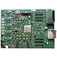
EVALUATION PLATFORM VIRTEX-5
Manufacturer
Xilinx Inc
Series
Virtex™-5 LXTr
Type
FPGAr
Datasheet
1.HW-V5-ML550-UNI-G.pdf
(88 pages)
Specifications of HW-V5-ML550-UNI-G
Contents
Development Platform, Power Supply, Loopback Board, CompactFlash Card, software and documentation
Silicon Manufacturer
Xilinx
Features
64M X 8 DDR SDRAM Memory, Six Samtec LVDS Connectors
Kit Contents
Board, Cable, PSU, CD, Docs
Silicon Family Name
Virtex-5
Silicon Core Number
XC5VLX50T-FFG1136
Rohs Compliant
Yes
Lead Free Status / RoHS Status
Lead free / RoHS Compliant
For Use With/related Products
Virtex™-5 LXT
Lead Free Status / RoHS Status
Lead free / RoHS Compliant, Lead free / RoHS Compliant
Available stocks
Company
Part Number
Manufacturer
Quantity
Price
Program Switch
USB Port (J22)
Table 3-8: RS-232 Interface Signal Names and Pin Assignments
ML550 Networking Interfaces Platform
UG202 (v1.4) April 18, 2008
Pin #
USB
J22
1
2
3
4
USB_VBUS
USB_D-
USB_D+
GND
Signal
USB
R
U2 Pin #
CP2102
USB I/F
8
5
4
3
The ML550 Development Board provides a push-button program switch (SW12) for
initiating the configuration of the Virtex-5 FPGA. This switch is used to force a
reconfiguration of the FPGA from PROMs if they are present and enabled. The ML550
Development Board does not include PROMs.
The primary configuration device is the System ACE Controller (U13), which loads image
files from a CompactFlash card. The mode DIP switch (SW11) must be set to the proper
mode for configuration to occur via the System ACE interface (refer to
Modes” on page 45
push button simply clears the FPGA configuration on this board.
The ML550 development board provides a USB “B” connector for interface to a PC (using
a USB B-to-A cable.) The board uses a Silicon Labs 3.3V CP2102 USB-to-RS232 converter
device (U2) to drive the RD, TD, RTS, and CTS signals to the FPGA via a Maxim MAX3008
level translator (U20). The user must provide a UART core internal to the FPGA to enable
serial communication. A Silicon Labs CP2102 driver file is included on the ML550
development kit CD. This driver allows a PC USB port to be configured as a serial COM
port for the user to continue working with serial communication utilities like
HyperTerminal or Tera Term Pro.
Table 3-8
assignments.
RS232 I/F
U2 Pin #
CP2102
28
27
26
25
24
23
12
describes the USB interface signal names and their respective Virtex-5 FPGA pin
9
USB_DTR_I_B
USB_DSR_I_B
USB_TX_O
USB_RX_I
USB_RTS_O_B
USB_CTS_I_B
USB_RESET_I_B
USB_SUSPEND_O
for further information regarding setting mode jumpers). The PROG
CP2102
RS232
Signal
www.xilinx.com
USB-Side
Pin #
U20
1
6
7
3
8
4
9
5
FPGA-Side
Pin #
14
18
13
17
12
16
20
15
U20
USB_DTR_B
USB_DSR_B
USB_TX
USB_RX
USB_RTS_B
USB_CTS_B
USB_RESET_B
USB_SUSPEND
U20 to FPGA
Signal Name
2.5V I/O
“Configuration
Program Switch
FPGA U9
Bank 11
C33
D34
B33
C34
A33
D32
B32
C32
Pin #
27


