ATICE50 Atmel, ATICE50 Datasheet - Page 28
ATICE50
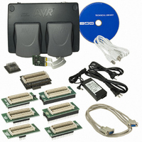
Manufacturer Part Number
ATICE50
Description
EMULATOR IN CIRCUIT MEGAAVR
Manufacturer
Atmel
Specifications of ATICE50
Lead Free Status / RoHS Status
Contains lead / RoHS non-compliant


2523A–AVR–11/02
General Description
3.5.3
3.5.4
3-14
Analog Comparator
A/D Converter
The Analog Comparator is built around a high speed comparator and a CMOS output
buffer/voltage converter. Figure 3-20 shows the Analog Comparator block diagram. The
total propagation delay from the AIN0 and AIN1 pins to the internal ACO signal is typi-
cally 90ns, max 210ns. For parts, the total propagation delay from the AIN0 and AIN1
pins to the internal ACO signal is typically 500 ns, max 750 ns.
The comparator features an internal hysteresis of typical 1 mV, max 4 mV @ 25 C to
ensure clean switching.
Figure 3-20. Analog Comparator Block Diagram
The block diagram of the ICE50 AD converter is shown in Figure 3-21.
Figure 3-21. ICE50 AD Converter
AVCC
ADC7
ADC6
ADC5
ADC4
ADC3
ADC2
ADC1
ADC0
2.5V
Aref
330Ω
330Ω
330Ω
330Ω
330Ω
330Ω
330Ω
330Ω
330Ω
330Ω
ACBG
ACME
ADEN
Pos
Input
Mux
Neg
Input
Mux
ADC Multiplexer
Output
AIN0
1.2V
AIN1
ADMUX Decoder
V
V
CC
CC
Aref Out
1.2V
ANALOG COMPARATOR
Voltage
Reference
Selection
A/D Converter
+
-
1x/10x/100x
+
-
+
-
ref
ADC Multiplexer Output
10K
ACD
10K
10K
10K
+
-
100R
+
-
1x/2x
ref
Vref
ACO
2
ICE50 User Guide
Vin
Vref
10-bit ADC
Q[0..9]
Related parts for ATICE50
Image
Part Number
Description
Manufacturer
Datasheet
Request
R

Part Number:
Description:
DEV KIT FOR AVR/AVR32
Manufacturer:
Atmel
Datasheet:

Part Number:
Description:
INTERVAL AND WIPE/WASH WIPER CONTROL IC WITH DELAY
Manufacturer:
ATMEL Corporation
Datasheet:
Part Number:
Description:
Low-Voltage Voice-Switched IC for Hands-Free Operation
Manufacturer:
ATMEL Corporation
Datasheet:
Part Number:
Description:
MONOLITHIC INTEGRATED FEATUREPHONE CIRCUIT
Manufacturer:
ATMEL Corporation
Datasheet:
Part Number:
Description:
AM-FM Receiver IC U4255BM-M
Manufacturer:
ATMEL Corporation
Datasheet:
Part Number:
Description:
Monolithic Integrated Feature Phone Circuit
Manufacturer:
ATMEL Corporation
Datasheet:
Part Number:
Description:
Multistandard Video-IF and Quasi Parallel Sound Processing
Manufacturer:
ATMEL Corporation
Datasheet:
Part Number:
Description:
High-performance EE PLD
Manufacturer:
ATMEL Corporation
Datasheet:
Part Number:
Description:
8-bit Flash Microcontroller
Manufacturer:
ATMEL Corporation
Datasheet:
Part Number:
Description:
2-Wire Serial EEPROM
Manufacturer:
ATMEL Corporation
Datasheet: