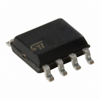
TL061ID STMicroelectronics, TL061ID Datasheet

TL061ID
Specifications of TL061ID
Available stocks
Related parts for TL061ID
TL061ID Summary of contents
Page 1
Features ■ Very low power consumption: 200 µA ■ Wide common-mode ( differential voltage ranges ■ Low input bias and offset currents ■ Output short-circuit protection ■ High input impedance JFET input stage ■ Internal frequency compensation ■ ...
Page 2
Schematic diagram 1 Schematic diagram Figure 1. Schematic diagram Inverting Non-inverting Input Input 4.2k Ω Offset Null 1 Offset Null 2 Figure 2. Input offset voltage null circuit 2/16 220 Ω 64 Ω Output 45k Ω 270 Ω 100 Ω ...
Page 3
TL061 2 Absolute maximum ratings and operating conditions Table 1. Absolute maximum ratings Symbol Parameter (1) V Supply voltage CC (2) V Input voltage i V Differential input voltage id P Power dissipation tot Output short-circuit duration T Storage temperature ...
Page 4
Electrical characteristics 3 Electrical characteristics Table ± amb Symbol Parameter Input offset voltage ( +25°C io amb ≤ T ≤ min amb max Temperature coefficient of input DV ...
Page 5
TL061 Table ± amb Symbol Parameter Overshoot factor (see 20mV 10kΩ Equivalent input noise voltage 100Ω ...
Page 6
Electrical characteristics Table ± amb Symbol Parameter Slew rate 10V 10kΩ Rise time 20mV 10kΩ ...
Page 7
TL061 Figure 3. Maximum peak-to-peak output voltage versus supply voltage Figure 5. Maximum peak-to-peak output voltage versus load resistance Figure 7. Differential voltage amplification versus free air temperature Electrical characteristics Figure 4. Maximum peak-to-peak output voltage versus free air temperature ...
Page 8
Electrical characteristics Figure 9. Supply current per amplifier versus supply voltage 250 200 150 100 SUPPLY VOLTAGE ( V) Figure 11. Total power dissipated versus free air temperature 30 V 15V = C ...
Page 9
TL061 Figure 15. Voltage follower large signal pulse response 6 INPUT 100pF amb - TIME (μs) Figure 17. Equivalent input noise voltage versus frequency 100 ...
Page 10
Parameter measurement information 4 Parameter measurement information Figure 18. Voltage follower 10/16 Figure 19. Gain-of-10 inverting amplifier 10k Ω 1k Ω TL061 R L TL061 100pF L ...
Page 11
TL061 5 Package information In order to meet environmental requirements, ST offers these devices in different grades of ® ECOPACK packages, depending on their level of environmental compliance. ECOPACK specifications, grade definitions and product status are available at: www.st.com. ® ...
Page 12
Package information 5.1 DIP8 package information Figure 20. DIP8 package mechanical drawing Table 5. DIP8 package mechanical data Ref 12/16 Dimensions Millimeters Min. Typ. Max. 5.33 0.38 ...
Page 13
TL061 5.2 SO-8 package information Figure 21. SO-8 package mechanical drawing Table 6. SO-8 package mechanical data Ref ccc Dimensions Millimeters Min. Typ. Max. 1.75 0.10 0.25 ...
Page 14
... Ordering information 6 Ordering information Table 7. Order codes Part number TL061MN TL061AMN TL061BMN TL061MD/MDT TL061AMD/MDT TL061BMD/BMDT TL061IN TL061AIN TL061BIN TL061ID/IDT TL061AID/AIDT TL061BID/BIDT TL061CN TL061ACN TL061BCN TL061CD/CDT TL061ACD/ACDT TL061BCD/BCDT 14/16 Temperature Package range DIP8 -55°C, +125°C SO-8 DIP8 -40°C, +105°C SO-8 DIP8 0° ...
Page 15
TL061 7 Revision history Table 8. Document revision history Date 13-Nov-2001 27-Jul-2007 05-Mar-2009 Revision 1 Initial release. Added values for R thja ratings. 2 Added Table 2: Operating Updated format. Updated package mechanical drawings and data in 3 Chapter 5: ...
Page 16
... Information in this document is provided solely in connection with ST products. STMicroelectronics NV and its subsidiaries (“ST”) reserve the right to make changes, corrections, modifications or improvements, to this document, and the products and services described herein at any time, without notice. All ST products are sold pursuant to ST’s terms and conditions of sale. ...


