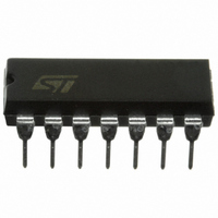
TL074BCN STMicroelectronics, TL074BCN Datasheet

TL074BCN
Specifications of TL074BCN
Available stocks
Related parts for TL074BCN
TL074BCN Summary of contents
Page 1
Features ■ Wide common-mode ( differential voltage range ■ Low input bias and offset current = 15 nV/ √Hz (typ) ■ Low noise e n ■ Output short-circuit protection ■ High input impedance JFET input stage ■ Low ...
Page 2
Schematic diagram 1 Schematic diagram Figure 1. Circuit schematics V CC Non-inverting input Inverting input V CC 2/15 1.3k 1.3k 35k 35k Ω Ω Ω 30k 8.2k Ω ...
Page 3
TL074 2 Absolute maximum ratings and operating conditions Table 1. Absolute maximum ratings Symbol (1) V Supply voltage CC (2) V Input voltage i V Differential input voltage id P Power dissipation tot Thermal resistance junction to ambient R DIP14 ...
Page 4
Electrical characteristics 3 Electrical characteristics Table ±15V amb Symbol Parameter Input offset voltage ( +25°C amb V io ≤ T ≤ min amb max DV Input offset voltage drift io ...
Page 5
TL074 Table ±15V amb Symbol Parameter Rise time 20mV 2kΩ gain Overshoot 20mV 2kΩ gain ...
Page 6
Electrical characteristics Figure 2. Maximum peak-to-peak output voltage versus frequency Figure 4. Maximum peak-to-peak output voltage versus frequency Figure 6. Maximum peak-to-peak output voltage versus load resistance 6/15 Figure 3. Maximum peak-to-peak output voltage versus frequency Figure 5. Maximum peak-to-peak ...
Page 7
TL074 Figure 8. Input bias current versus free air temperature 100 V 15V = 0.1 0.01 -50 - TEMPERATURE (˚C) Figure 10. Large signal differential voltage amplification and phase shift versus frequency W Figure 12. ...
Page 8
Electrical characteristics Figure 14. Voltage follower large signal pulse response Figure 16. Equivalent input noise voltage versus frequency 100 400 1k FREQUENCY (Hz) 8/15 Figure ...
Page 9
TL074 4 Parameter measurement information Figure 18. Voltage follower Parameter measurement information Figure 19. Gain-of-10 inverting amplifier 10k Ω 1k Ω 1/4 TL074 100pF L 9/15 ...
Page 10
Typical applications 5 Typical applications Figure 20. Audio distribution amplifier 1M Ω 1 μ F Input 100k Ω 1OO μ F Figure 21. Positive feeback bandpass filter 43k Ω 43k Ω Input - 1 ...
Page 11
TL074 Figure 22. Output A SECOND ORDER BANDPASS FILTER fo = 100 kHz 30; Gain = 16 Figure 23. Output B CASCADED BANDPASS FILTER fo = 100 kHz 69; Gain = 16 Typical applications 11/15 ...
Page 12
Package information 6 Package information In order to meet environmental requirements, ST offers these devices in ECOPACK® packages. These packages have a lead-free second level interconnect. The category of second level interconnect is marked on the package and on the ...
Page 13
TL074 6.2 SO-14 package information Figure 25. SO-14 package mechanical drawing Table 5. SO-14 package mechanical data Ref Dimensions Millimeters Min. Typ. Max. 1.75 ...
Page 14
... Added automotive grade order codes in Packing Marking TL074IN Tube TL074AIN TL074BIN Tube or tape & reel Tube or 074AIY tape & reel 074BIY TL074CN Tube TL074ACN TL074BCN Tube or tape & reel Changes , R and ESD in Table 1: Absolute maximum thjc conditions. codes. Table 6: Order codes. TL074 074I 074AI 074BI ...
Page 15
... TL074 Information in this document is provided solely in connection with ST products. STMicroelectronics NV and its subsidiaries (“ST”) reserve the right to make changes, corrections, modifications or improvements, to this document, and the products and services described herein at any time, without notice. All ST products are sold pursuant to ST’s terms and conditions of sale. ...


