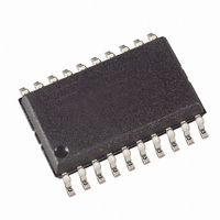
AT89LP2052-20SU Atmel, AT89LP2052-20SU Datasheet - Page 22

AT89LP2052-20SU
Manufacturer Part Number
AT89LP2052-20SU
Description
IC 8051 MCU FLASH 2K 20SOIC
Manufacturer
Atmel
Series
89LPr
Datasheet
1.AT89LP2052-20PU.pdf
(94 pages)
Specifications of AT89LP2052-20SU
Core Processor
8051
Core Size
8-Bit
Speed
20MHz
Connectivity
SPI, UART/USART
Peripherals
Brown-out Detect/Reset, POR, PWM, WDT
Number Of I /o
15
Program Memory Size
2KB (2K x 8)
Program Memory Type
FLASH
Ram Size
256 x 8
Voltage - Supply (vcc/vdd)
2.4 V ~ 5.5 V
Oscillator Type
Internal
Operating Temperature
-40°C ~ 85°C
Package / Case
20-SOIC (7.5mm Width)
Processor Series
AT89x
Core
8051
Data Bus Width
8 bit
Data Ram Size
256 B
Interface Type
UART, SPI
Maximum Clock Frequency
20 MHz
Number Of Programmable I/os
15
Number Of Timers
2
Operating Supply Voltage
2.4 V to 5.5 V
Maximum Operating Temperature
+ 85 C
Mounting Style
SMD/SMT
3rd Party Development Tools
PK51, CA51, A51, ULINK2
Development Tools By Supplier
AT89ISP
Minimum Operating Temperature
- 40 C
Package
20SOIC W
Device Core
8051
Family Name
AT89
Maximum Speed
20 MHz
Lead Free Status / RoHS Status
Lead free / RoHS Compliant
Eeprom Size
-
Data Converters
-
Lead Free Status / Rohs Status
Details
15.3
15.4
15.5
22
Open-drain Output
Push-pull Output
Port 1 Analog Functions
AT89LP2052/LP4052
The open-drain output configuration turns off all pull-ups and only drives the pull-down transistor
of the port pin when the port register contains a logic “0”. To be used as a logic output, a port
configured in this manner must have an external pull-up, typically a resistor tied to V
down for this mode is the same as for the quasi-bidirectional mode. The open-drain port configu-
ration is shown in
down (see
Figure 15-4. Open-Drain Output
The push-pull output configuration has the same pull-down structure as both the open-drain and
the quasi-bidirectional output modes, but provides a continuous strong pull-up when the port
register contains a logic “1”. The push-pull mode may be used when more source current is
needed from a port output. The push-pull port configuration is shown in
circuitry of P3.2 and P3.3 is not disabled during Power-down (see
Figure 15-5. Push-pull Output
The AT89LP2052/LP4052 incorporates an analog comparator. In order to give the best analog
performance and minimize power consumption, pins that are being used for analog functions
must have both the digital outputs and digital inputs disabled. Digital outputs are disabled by put-
ting the port pins into the input-only mode as described in
Digital inputs on P1.0 and P1.1 are disabled whenever the Analog Comparator is enabled by
setting the CEN bit in ACSR. CEN forces the PWD input on P1.0 and P1.1 low, thereby disabling
the Schmitt trigger circuitry.
Figure
From Port
Register
From Port
Register
Figure
15-3).
15-4. The input circuitry of P3.2 and P3.3 is not disabled during Power-
Input
Input
Data
Data
PWD
PWD
V
CC
Section 15. “I/O Ports” on page
Figure
Figure
15-3).
Port
Port
Pin
Pin
3547J–MICRO–10/09
15-5. The input
CC
. The pull-
20.


