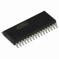
AT90PWM3B-16SU Atmel, AT90PWM3B-16SU Datasheet - Page 244

AT90PWM3B-16SU
Manufacturer Part Number
AT90PWM3B-16SU
Description
IC MCU AVR RISC 8K FLASH 32-SOIC
Manufacturer
Atmel
Series
AVR® 90PWM Lightingr
Specifications of AT90PWM3B-16SU
Core Processor
AVR
Core Size
8-Bit
Speed
16MHz
Connectivity
SPI, UART/USART
Peripherals
Brown-out Detect/Reset, POR, PWM, WDT
Number Of I /o
27
Program Memory Size
8KB (8K x 8)
Program Memory Type
FLASH
Eeprom Size
512 x 8
Ram Size
512 x 8
Voltage - Supply (vcc/vdd)
2.7 V ~ 5.5 V
Data Converters
A/D 11x10b; D/A 1x10b
Oscillator Type
Internal
Operating Temperature
-40°C ~ 105°C
Package / Case
32-SOIC (7.5mm Width)
Processor Series
AT90PWMx
Core
AVR8
Data Bus Width
8 bit
Data Ram Size
512 B
Interface Type
SPI/USART
Maximum Clock Frequency
16 MHz
Number Of Programmable I/os
27
Number Of Timers
2
Operating Supply Voltage
2.7 V to 5.5 V
Maximum Operating Temperature
+ 105 C
Mounting Style
SMD/SMT
3rd Party Development Tools
EWAVR, EWAVR-BL
Development Tools By Supplier
ATAVRDRAGON, ATSTK500, ATSTK600, ATAVRISP2, ATAVRONEKIT, ATAVRFBKIT, ATAVRISP2
Minimum Operating Temperature
- 40 C
On-chip Adc
11-ch x 10-bit
On-chip Dac
1-chx10-bit
Controller Family/series
AVR PWM
Eeprom Memory Size
512Byte
Ram Memory Size
512Byte
Cpu Speed
16MHz
Rohs Compliant
Yes
For Use With
ATSTK600-SOIC - STK600 SOCKET/ADAPTER FOR SOIC770-1007 - ISP 4PORT ATMEL AVR MCU SPI/JTAGATAVRMC200 - KIT EVAL FOR AT90PWM3 ASYNCATAVRFBKIT - KIT DEMO BALLAST FOR AT90PWM2ATAVRISP2 - PROGRAMMER AVR IN SYSTEMATSTK520 - ADAPTER KIT FOR 90PWM
Lead Free Status / RoHS Status
Lead free / RoHS Compliant
Available stocks
Company
Part Number
Manufacturer
Quantity
Price
Company:
Part Number:
AT90PWM3B-16SU
Manufacturer:
Atmel
Quantity:
4 000
Part Number:
AT90PWM3B-16SU
Manufacturer:
MICROCHIP/微芯
Quantity:
20 000
- Current page: 244 of 361
- Download datasheet (7Mb)
21.7
244
ADC Conversion Result
AT90PWM2/3/2B/3B
Figure 21-13. Differential Non-linearity (DNL)
•
•
After the conversion is complete (ADIF is high), the conversion result can be found in the ADC
Result Registers (ADCL, ADCH).
For single ended conversion, the result is:
where V
Table 21-3 on page 246
0x3FF represents the selected reference voltage.
If differential channels are used, the result is:
where V
GAIN the selected gain factor and V
in two’s complement form, from 0x200 (-512d) through 0x1FF (+511d). Note that if the user
wants to perform a quick polarity check of the result, it is sufficient to read the MSB of the result
(ADC9 in ADCH). If the bit is one, the result is negative, and if this bit is zero, the result is posi-
tive.
Table 82 shows the resulting output codes if the differential input channel pair (ADCn - ADCm) is
selected with a reference voltage of V
Quantization Error: Due to the quantization of the input voltage into a finite number of codes,
a range of input voltages (1 LSB wide) will code to the same value. Always ± 0.5 LSB.
Absolute Accuracy: The maximum deviation of an actual (unadjusted) transition compared
to an ideal transition for any code. This is the compound effect of offset, gain error,
differential error, non-linearity, and quantization error. Ideal value: ± 0.5 LSB.
Figure 21-14
IN
POS
is the voltage on the selected input pin and V
is the voltage on the positive input pin, V
Output Code
shows the decoding of the differential input range.
0x000
0x3FF
and
0
Table 21-4 on page
1 LSB
ADC
REF
REF
ADC
=
the selected voltage reference. The result is presented
.
(
----------------------------------------------------------------------- -
V
=
POS
V
--------------------------
IN
V
–
⋅
REF
247). 0x000 represents analog ground, and
V
1023
NEG
NEG
V
REF
REF
) GAIN 512
⋅
the voltage on the negative input pin,
the selected voltage reference (see
⋅
V
REF
Input Voltage
4317J–AVR–08/10
Related parts for AT90PWM3B-16SU
Image
Part Number
Description
Manufacturer
Datasheet
Request
R

Part Number:
Description:
Manufacturer:
Atmel Corporation
Datasheet:

Part Number:
Description:
IC MCU AVR RISC 8K FLASH 32-QFN
Manufacturer:
Atmel
Datasheet:

Part Number:
Description:
MCU AVR 8K FLASH 16MHA 32SOIC
Manufacturer:
Atmel
Datasheet:

Part Number:
Description:
IC AVR MCU FLASH 8K 32QFN
Manufacturer:
Atmel
Datasheet:

Part Number:
Description:
IC AVR MCU FLASH 8K 32SOIC
Manufacturer:
Atmel
Datasheet:

Part Number:
Description:
MCU AVR 8K FLASH 16MHZ 32-QFN
Manufacturer:
Atmel
Datasheet:

Part Number:
Description:
DEV KIT FOR AVR/AVR32
Manufacturer:
Atmel
Datasheet:

Part Number:
Description:
INTERVAL AND WIPE/WASH WIPER CONTROL IC WITH DELAY
Manufacturer:
ATMEL Corporation
Datasheet:

Part Number:
Description:
Low-Voltage Voice-Switched IC for Hands-Free Operation
Manufacturer:
ATMEL Corporation
Datasheet:

Part Number:
Description:
MONOLITHIC INTEGRATED FEATUREPHONE CIRCUIT
Manufacturer:
ATMEL Corporation
Datasheet:

Part Number:
Description:
AM-FM Receiver IC U4255BM-M
Manufacturer:
ATMEL Corporation
Datasheet:

Part Number:
Description:
Monolithic Integrated Feature Phone Circuit
Manufacturer:
ATMEL Corporation
Datasheet:

Part Number:
Description:
Multistandard Video-IF and Quasi Parallel Sound Processing
Manufacturer:
ATMEL Corporation
Datasheet:


