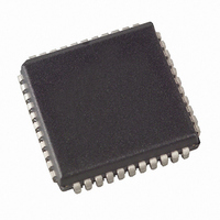
AT89C51RE2-SLSUM Atmel, AT89C51RE2-SLSUM Datasheet - Page 167

AT89C51RE2-SLSUM
Manufacturer Part Number
AT89C51RE2-SLSUM
Description
MCU 8BIT FLASH 2.7-5.5V 44-PLCC
Manufacturer
Atmel
Series
89Cr
Datasheet
1.AT89C51RE2-SLSUM.pdf
(187 pages)
Specifications of AT89C51RE2-SLSUM
Core Processor
8051
Core Size
8-Bit
Speed
60MHz
Connectivity
I²C, SPI, UART/USART
Peripherals
POR, PWM, WDT
Number Of I /o
34
Program Memory Size
128KB (128K x 8)
Program Memory Type
FLASH
Ram Size
8K x 8
Voltage - Supply (vcc/vdd)
2.7 V ~ 5.5 V
Oscillator Type
External
Operating Temperature
-40°C ~ 85°C
Package / Case
44-PLCC
Package
44PLCC
Device Core
8051
Family Name
89C
Maximum Speed
40 MHz
Operating Supply Voltage
3.3|5 V
Data Bus Width
8 Bit
Number Of Programmable I/os
34
Interface Type
SPI/TWI/UART
Number Of Timers
3
Processor Series
AT89x
Core
8051
Data Ram Size
8 KB
Maximum Clock Frequency
40 MHz
Maximum Operating Temperature
+ 85 C
Mounting Style
SMD/SMT
3rd Party Development Tools
PK51, CA51, A51, ULINK2
Development Tools By Supplier
AT89OCD-01
Minimum Operating Temperature
- 40 C
Cpu Family
89C
Device Core Size
8b
Frequency (max)
40MHz
Total Internal Ram Size
8KB
# I/os (max)
34
Number Of Timers - General Purpose
3
Operating Supply Voltage (typ)
3.3/5V
Operating Supply Voltage (max)
5.5V
Operating Supply Voltage (min)
2.7V
Instruction Set Architecture
CISC
Operating Temp Range
-40C to 85C
Operating Temperature Classification
Industrial
Mounting
Surface Mount
Pin Count
44
Package Type
PLCC
For Use With
AT89OCD-01 - USB EMULATOR FOR AT8XC51 MCUAT89STK-11 - KIT STARTER FOR AT89C51RX2
Lead Free Status / RoHS Status
Lead free / RoHS Compliant
Eeprom Size
-
Data Converters
-
Lead Free Status / Rohs Status
Lead free / RoHS Compliant
Available stocks
Company
Part Number
Manufacturer
Quantity
Price
Company:
Part Number:
AT89C51RE2-SLSUM
Manufacturer:
HONEYWELL
Quantity:
101
T
Notes:
7663E–8051–10/08
A
Symbol
= -40°C to +85°C; V
I
I
CCWRITE
t
I
CCIDLE
R
WRITE
CCOP
C
I
I
I
I
RST
PD
TL
IL
LI
IO
1. Operating I
2. Idle I
3. Power-down I
4. Capacitance loading on Ports 0 and 2 may cause spurious noise pulses to be superimposed on the V
5. Typical values are based on a limited number of samples and are not guaranteed. The values listed are at room temperature
6. Under steady state (non-transient) conditions, I
V
(see Figure 71).
0.5V; XTAL2 N.C; Port 0 = V
ure 73).
and 3. The noise is due to external bus capacitance discharging into the Port 0 and Port 2 pins when these pins make 1 to 0
transitions during bus operation. In the worst cases (capacitive loading 100 pF), the noise pulse on the ALE line may exceed
0.45V with maxi V
and 5V.
Maximum I
Maximum I
Port 0: 26 mA
Ports 1, 2 and 3: 15 mA
Maximum total I
If I
than the listed test conditions.
Parameter
RST Pull-down Resistor
Logical 0 Input Current ports 1, 2, 3, 4 and 5
Input Leakage Current
Logical 1 to 0 Transition Current, ports 1, 2, 3, 4
Capacitance of I/O Buffer
Power-down Current
Power Supply Current on normal mode
Power Supply Current on idle mode
Power Supply Current on flash write
Flash programming time
SS
OL
+ 0.5V, V
CC
exceeds the test condition, V
is measured with all output pins disconnected; XTAL1 driven with T
OL
OL
CC
SS
IH
CC
per port pin: 10 mA
per 8-bit port:
is measured with all output pins disconnected; XTAL1 driven with T
= 0V; V
= V
OL
is measured with all output pins disconnected; EA = V
Figure 71. I
OL
for all output pins: 71 mA
CC
peak 0.6V. A Schmitt Trigger use is not necessary.
- 0.5V; XTAL2 N.C.; EA = RST = Port 0 = V
CC
=2.7V to 5.5V; F = 0 to 40 MHz (Continued)
CC
; EA = RST = V
CC
CLOCK
SIGNAL
Test Condition, Active Mode
OL
(NC)
may exceed the related specification. Pins are not guaranteed to sink current greater
V
CC
SS
OL
RST
XTAL2
XTAL1
V
(see Figure 72).
SS
must be externally limited as follows:
Min
50
V
EA
CC
I
P0
CC
V
200
Typ
CC
75
V
7
CC
(5)
CC
. I
0.8 x Frequency (MHz) + 15
0.4 x Frequency (MHz) + 5
0.3 x Frequency (MHz) + 5
CC
CC
, PORT 0 = V
would be slightly higher if a crystal oscillator used
CLCH
All other pins are disconnected.
, T
Max
-650
250
± 10
150
-50
10
10
CLCH
CHCL
, T
CC
= 5 ns, V
; XTAL2 NC.; RST = V
CHCL
= 5 ns (see Figure 74), V
AT89C51RE2
IL
Unit
= V
mA
mA
mA
ms
k Ω
μ A
μ A
μ A
pF
μ A
OLS
SS
of ALE and Ports 1
Test Conditions
V
0.45V < V
V
F
T
2.7 < V
V
V
V
2.7 < V
+ 0.5V, V
A
IN
IN
C
CC
CC
CC
= 25 ° C
= 3 MHz
= 0.45V
= 2.0V
= 5.5V
= 5.5V
= 5.5V
CC <
CC <
SS
IN
IH
(see Fig-
(1)
(2)
5.5V
5.5V
< V
= V
CC
(3)
167
CC
IL
=
-


