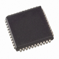
AT89C51RE2-SLSUM Atmel, AT89C51RE2-SLSUM Datasheet - Page 33

AT89C51RE2-SLSUM
Manufacturer Part Number
AT89C51RE2-SLSUM
Description
MCU 8BIT FLASH 2.7-5.5V 44-PLCC
Manufacturer
Atmel
Series
89Cr
Datasheet
1.AT89C51RE2-SLSUM.pdf
(187 pages)
Specifications of AT89C51RE2-SLSUM
Core Processor
8051
Core Size
8-Bit
Speed
60MHz
Connectivity
I²C, SPI, UART/USART
Peripherals
POR, PWM, WDT
Number Of I /o
34
Program Memory Size
128KB (128K x 8)
Program Memory Type
FLASH
Ram Size
8K x 8
Voltage - Supply (vcc/vdd)
2.7 V ~ 5.5 V
Oscillator Type
External
Operating Temperature
-40°C ~ 85°C
Package / Case
44-PLCC
Package
44PLCC
Device Core
8051
Family Name
89C
Maximum Speed
40 MHz
Operating Supply Voltage
3.3|5 V
Data Bus Width
8 Bit
Number Of Programmable I/os
34
Interface Type
SPI/TWI/UART
Number Of Timers
3
Processor Series
AT89x
Core
8051
Data Ram Size
8 KB
Maximum Clock Frequency
40 MHz
Maximum Operating Temperature
+ 85 C
Mounting Style
SMD/SMT
3rd Party Development Tools
PK51, CA51, A51, ULINK2
Development Tools By Supplier
AT89OCD-01
Minimum Operating Temperature
- 40 C
Cpu Family
89C
Device Core Size
8b
Frequency (max)
40MHz
Total Internal Ram Size
8KB
# I/os (max)
34
Number Of Timers - General Purpose
3
Operating Supply Voltage (typ)
3.3/5V
Operating Supply Voltage (max)
5.5V
Operating Supply Voltage (min)
2.7V
Instruction Set Architecture
CISC
Operating Temp Range
-40C to 85C
Operating Temperature Classification
Industrial
Mounting
Surface Mount
Pin Count
44
Package Type
PLCC
For Use With
AT89OCD-01 - USB EMULATOR FOR AT8XC51 MCUAT89STK-11 - KIT STARTER FOR AT89C51RX2
Lead Free Status / RoHS Status
Lead free / RoHS Compliant
Eeprom Size
-
Data Converters
-
Lead Free Status / Rohs Status
Lead free / RoHS Compliant
Available stocks
Company
Part Number
Manufacturer
Quantity
Price
Company:
Part Number:
AT89C51RE2-SLSUM
Manufacturer:
HONEYWELL
Quantity:
101
FM0 Memory
Architecture
User Space
Extra Row (XRow or
XAF)
Hardware security Byte
(HSB)
7663E–8051–10/08
The FM0 flash memory is made up of 5 blocks:
1. The memory array (user space) 128K bytes
2. The Extra Row also called FM0 XAF
3. The Hardware security bits (HSB)
4. The Fuse Configuration Byte (FCB)
5. The column latch
This space is composed of a 128K bytes Flash memory organized in 1024 pages of 128 bytes. It
contains the user’s application code. This block can be access in Read/write mode from FM0
and boot memory area. (When access in write mode from FM0, the CPU core enter pseudo idle
mode).
This row is a part of FM0 and has a size of 128 bytes. The extra row (XAF) may contain informa-
tion for boot loader usage.This block can be access in Read/write mode from FM0 and boot
memory area. (When access in write mode from FM0, the CPU core enter pseudo idle mode).
The Hardware security Byte is a part of FM0 and has a size of 1 byte.
The 8 bits can be read/written by software (from FM0 or RM0) and written by hardware in paral-
lel mode.
The HSB bits can be written to ‘0’ without any restriction (increase the security level of the chip),
but can be written to ‘1’ only when the corresponding memory area of the lock bits was full chip
erased.
Table 19. Hardware Security Byte (HSB)
Number
Bit
6-4
2-0
7
3
7
-
Mnemonic
FLB2-0
Bit
-
-
-
6
-
Description
Unused
Reserved
Unused
FM0 Memory Lock Bits
See Table 32 on page 52
5
-
4
-
3
-
FLB2
2
AT89C51RE2
FLB1
1
FLB0
0
33


