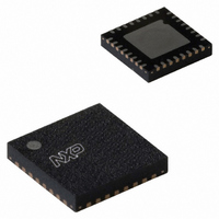
LPC1114FHN33/301,5 NXP Semiconductors, LPC1114FHN33/301,5 Datasheet - Page 35

LPC1114FHN33/301,5
Manufacturer Part Number
LPC1114FHN33/301,5
Description
IC MCU 32BIT 32KB FLASH 33HVQFN
Manufacturer
NXP Semiconductors
Series
LPC1100r
Datasheets
1.LPC1114FHN333015.pdf
(2 pages)
2.LPC1114FHN333015.pdf
(66 pages)
3.LPC1114FHN333015.pdf
(66 pages)
Specifications of LPC1114FHN33/301,5
Program Memory Type
FLASH
Program Memory Size
32KB (32K x 8)
Package / Case
33-VQFN Exposed Pad, 33-HVQFN, 33-SQFN, 33-DHVQFN
Core Processor
ARM Cortex-M0
Core Size
32-Bit
Speed
50MHz
Connectivity
I²C, SPI, UART/USART
Peripherals
Brown-out Detect/Reset, POR, WDT
Number Of I /o
28
Ram Size
8K x 8
Voltage - Supply (vcc/vdd)
1.8 V ~ 3.6 V
Data Converters
A/D 8x10b
Oscillator Type
Internal
Operating Temperature
-40°C ~ 85°C
Processor Series
LPC11
Core
ARM Cortex M0
Data Bus Width
32 bit
Data Ram Size
8 KB
Interface Type
I2C, SPI, UART
Number Of Programmable I/os
28
Operating Supply Voltage
1.8 V to 3.6 V
Maximum Operating Temperature
+ 85 C
Mounting Style
SMD/SMT
3rd Party Development Tools
MDK-ARM, RL-ARM, ULINK2, KSK-LPC1114
Development Tools By Supplier
OM11049, OM11085
Minimum Operating Temperature
- 40 C
On-chip Adc
10 bit, 8 Channel
Package
33HVQFN EP
Device Core
ARM Cortex M0
Family Name
LPC1100
Maximum Speed
50 MHz
Number Of Timers
4
Lead Free Status / RoHS Status
Lead free / RoHS Compliant
For Use With
622-1005 - USB IN-CIRCUIT PROG ARM7 LPC2K
Eeprom Size
-
Lead Free Status / Rohs Status
Lead free / RoHS Compliant
Other names
568-4948
935290792551
935290792551
Available stocks
Company
Part Number
Manufacturer
Quantity
Price
Company:
Part Number:
LPC1114FHN33/301,5
Manufacturer:
NXP
Quantity:
1 300
NXP Semiconductors
[1]
[2]
[3]
[4]
[5]
[6]
[7]
[8]
[9]
[10] Low-current mode PWR_LOW_CURRENT selected when running the set_power routine in the power profiles.
[11] Including voltage on outputs in 3-state mode.
[12] V
[13] 3-state outputs go into 3-state mode in Deep power-down mode.
[14] Allowed as long as the current limit does not exceed the maximum current allowed by the device.
[15] To V
Table 8.
T
[1]
[2]
[3]
[4]
[5]
[6]
[7]
[8]
LPC1111_12_13_14
Product data sheet
Symbol
V
C
E
E
E
E
E
R
R
amb
IA
D
L(adj)
O
G
T
ia
vsi
i
Typical ratings are not guaranteed. The values listed are at room temperature (25 °C), nominal supply voltages.
T
I
IRC enabled; system oscillator disabled; system PLL disabled.
BOD disabled.
All peripherals disabled in the SYSAHBCLKCTRL register. Peripheral clocks to UART and SPI0/1 disabled in system configuration
block.
IRC disabled; system oscillator enabled; system PLL enabled.
All oscillators and analog blocks turned off in the PDSLEEPCFG register; PDSLEEPCFG = 0x0000 18FF.
WAKEUP pin pulled HIGH externally.
The ADC is monotonic, there are no missing codes.
The differential linearity error (E
The integral non-linearity (E
appropriate adjustment of gain and offset errors. See
The offset error (E
ideal curve. See
The gain error (E
error, and the straight line which fits the ideal transfer curve. See
The absolute error (E
ADC and the ideal transfer curve. See
T
Input resistance R
DD
= −40 °C to +85 °C unless otherwise specified; ADC frequency 4.5 MHz, V
amb
amb
DD
measurements were performed with all pins configured as GPIO outputs driven LOW and pull-up resistors disabled.
SS
supply voltage must be present.
= 25 °C.
= 25 °C; maximum sampling frequency f
.
ADC static characteristics
Parameter
analog input voltage
analog input capacitance
differential linearity error
integral non-linearity
offset error
gain error
absolute error
voltage source interface
resistance
input resistance
Figure
G
i
O
) is the relative difference in percent between the straight line fitting the actual transfer curve after removing offset
depends on the sampling frequency fs: R
) is the absolute difference between the straight line which fits the actual curve and the straight line which fits the
T
) is the maximum difference between the center of the steps of the actual transfer curve of the non-calibrated
7.
L(adj)
D
) is the peak difference between the center of the steps of the actual and the ideal transfer curve after
) is the difference between the actual step width and the ideal step width. See
Figure
All information provided in this document is subject to legal disclaimers.
Conditions
s
7.
= 4.5 MHz and analog input capacitance C
Rev. 4 — 10 February 2011
Figure
i
7.
= 1 / (f
Figure
s
× C
7.
ia
).
[1][2]
[7][8]
[3]
[4]
[5]
[6]
Min
0
-
-
-
-
-
-
-
-
32-bit ARM Cortex-M0 microcontroller
DD
= 2.5 V to 3.6 V.
LPC1111/12/13/14
ia
= 1 pF.
Typ
-
-
-
-
-
-
-
-
-
Max
V
1
± 1
± 1.5
± 3.5
0.6
± 4
40
2.5
Figure
© NXP B.V. 2011. All rights reserved.
DD
7.
Unit
V
pF
LSB
LSB
LSB
%
LSB
kΩ
MΩ
35 of 66


