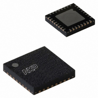
LPC1114FHN33/301,5 NXP Semiconductors, LPC1114FHN33/301,5 Datasheet - Page 53

LPC1114FHN33/301,5
Manufacturer Part Number
LPC1114FHN33/301,5
Description
IC MCU 32BIT 32KB FLASH 33HVQFN
Manufacturer
NXP Semiconductors
Series
LPC1100r
Datasheets
1.LPC1114FHN333015.pdf
(2 pages)
2.LPC1114FHN333015.pdf
(66 pages)
3.LPC1114FHN333015.pdf
(66 pages)
Specifications of LPC1114FHN33/301,5
Program Memory Type
FLASH
Program Memory Size
32KB (32K x 8)
Package / Case
33-VQFN Exposed Pad, 33-HVQFN, 33-SQFN, 33-DHVQFN
Core Processor
ARM Cortex-M0
Core Size
32-Bit
Speed
50MHz
Connectivity
I²C, SPI, UART/USART
Peripherals
Brown-out Detect/Reset, POR, WDT
Number Of I /o
28
Ram Size
8K x 8
Voltage - Supply (vcc/vdd)
1.8 V ~ 3.6 V
Data Converters
A/D 8x10b
Oscillator Type
Internal
Operating Temperature
-40°C ~ 85°C
Processor Series
LPC11
Core
ARM Cortex M0
Data Bus Width
32 bit
Data Ram Size
8 KB
Interface Type
I2C, SPI, UART
Number Of Programmable I/os
28
Operating Supply Voltage
1.8 V to 3.6 V
Maximum Operating Temperature
+ 85 C
Mounting Style
SMD/SMT
3rd Party Development Tools
MDK-ARM, RL-ARM, ULINK2, KSK-LPC1114
Development Tools By Supplier
OM11049, OM11085
Minimum Operating Temperature
- 40 C
On-chip Adc
10 bit, 8 Channel
Package
33HVQFN EP
Device Core
ARM Cortex M0
Family Name
LPC1100
Maximum Speed
50 MHz
Number Of Timers
4
Lead Free Status / RoHS Status
Lead free / RoHS Compliant
For Use With
622-1005 - USB IN-CIRCUIT PROG ARM7 LPC2K
Eeprom Size
-
Lead Free Status / Rohs Status
Lead free / RoHS Compliant
Other names
568-4948
935290792551
935290792551
Available stocks
Company
Part Number
Manufacturer
Quantity
Price
Company:
Part Number:
LPC1114FHN33/301,5
Manufacturer:
NXP
Quantity:
1 300
NXP Semiconductors
Table 18.
[1]
[2]
[3]
[4]
LPC1111_12_13_14
Product data sheet
Symbol
T
t
t
t
t
DS
DH
v(Q)
h(Q)
cy(PCLK)
T
main clock frequency f
and the SPI CPSDVSR parameter (specified in the SPI clock prescale register).
T
T
T
cy(clk)
amb
cy(clk)
amb
= −40 °C to 85 °C.
= 25 °C; for normal voltage supply range: V
= (SSPCLKDIV × (1 + SCR) × CPSDVSR) / f
= 12 × T
Dynamic characteristics of SPI pins in SPI mode
Parameter
PCLK cycle time
data set-up time
data hold time
data output valid time in SPI mode
data output hold time in SPI mode
cy(PCLK)
main
.
Fig 28. SPI master timing in SPI mode
, the SPI peripheral clock divider (SSPCLKDIV), the SPI SCR parameter (specified in the SSP0CR0 register),
SCK (CPOL = 0)
SCK (CPOL = 1)
Conditions
in SPI mode
in SPI mode
Pin names SCK, MISO, and MOSI refer to pins for both SPI peripherals, SPI0 and SPI1.
MOSI
MISO
MOSI
MISO
All information provided in this document is subject to legal disclaimers.
DD
Rev. 4 — 10 February 2011
main
= 3.3 V.
DATA VALID
DATA VALID
. The clock cycle time derived from the SPI bit rate T
t
v(Q)
[3][4]
[3][4]
[3][4]
[3][4]
DATA VALID
T
DATA VALID
cy(clk)
Min
20
0
3 × T
-
-
t
v(Q)
t
DS
DATA VALID
cy(PCLK)
DATA VALID
t
clk(H)
t
t
DH
DS
32-bit ARM Cortex-M0 microcontroller
+ 4
DATA VALID
DATA VALID
LPC1111/12/13/14
Typ
-
-
-
-
-
t
clk(L)
t
DH
t
h(Q)
Max
-
-
3 × T
2 × T
-
t
cy(PCLK)
cy(PCLK)
h(Q)
cy(clk)
© NXP B.V. 2011. All rights reserved.
is a function of the
+ 11
+ 5
CPHA = 1
CPHA = 0
002aae829
53 of 66
Unit
ns
ns
ns
ns
ns


