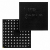
LPC3240FET296/01,5 NXP Semiconductors, LPC3240FET296/01,5 Datasheet - Page 10

LPC3240FET296/01,5
Manufacturer Part Number
LPC3240FET296/01,5
Description
IC ARM9 MCU 256K 296-TFBGA
Manufacturer
NXP Semiconductors
Series
LPC32x0r
Specifications of LPC3240FET296/01,5
Package / Case
296-TFBGA
Core Processor
ARM9
Core Size
16/32-Bit
Speed
266MHz
Connectivity
EBI/EMI, Ethernet, I²C, IrDA, Microwire, SPI, SSI, SSP, UART/USART, USB OTG
Peripherals
DMA, I²S, Motor Control PWM, PWM, WDT
Number Of I /o
51
Program Memory Type
ROMless
Ram Size
256K x 8
Voltage - Supply (vcc/vdd)
0.9 V ~ 3.6 V
Data Converters
A/D 3x10b
Oscillator Type
Internal
Operating Temperature
-40°C ~ 85°C
Processor Series
LPC32
Core
ARM926EJ-S
Data Bus Width
32 bit
Data Ram Size
256 KB
Interface Type
EMC
Maximum Clock Frequency
266 MHz
Number Of Timers
6
Operating Supply Voltage
1.31 V to 1.39 V
Maximum Operating Temperature
+ 85 C
Mounting Style
SMD/SMT
3rd Party Development Tools
MDK-ARM, RL-ARM, ULINK2
Minimum Operating Temperature
- 40 C
On-chip Adc
10 bit, 3 Channel
Lead Free Status / RoHS Status
Lead free / RoHS Compliant
Eeprom Size
-
Program Memory Size
-
Lead Free Status / Rohs Status
Lead free / RoHS Compliant
Other names
568-4963
935290765551
935290765551
Available stocks
Company
Part Number
Manufacturer
Quantity
Price
Company:
Part Number:
LPC3240FET296/01,5
Manufacturer:
NXP
Quantity:
630
Company:
Part Number:
LPC3240FET296/01,5
Manufacturer:
NXP Semiconductors
Quantity:
10 000
NXP Semiconductors
ES_LPC3240
Errata sheet
Fig 5.
128 MB DDR SDRAM example
LPC32x0 EMC
Example 128 MB system DDR SDRAM using a single EMC_DYCSx_N:
EMC_DYCS0_N
5. The PCB trace length of EMC_DQS[1:0] should be at least 2 inches (but not more
EMC_D[07:00]
EMC_A[14:00]
EMC_D[15:08]
EMC_Control
EMC_CLK_N
EMC_CLKIN
EMC_DQM0
EMC_DQS0
EMC_DQS1
EMC_DQM1
EMC_CLK
than 4 inches) longer than EMC_DQ[15:0] and EMC_DQM[1:0]. On a typical FR4
PCB this adds at least 334 ps to set-up time margin for DDR writes. For reads from
DDR the increased trace length of EMC_DQS[1:0] will be automatically compensated
for by the software initialization function find_ddr_dqsin_delay() which sets the optimal
value DDR_DQSIN_DELAY(SDRAMCLK_CTRL[6:2]). The function
find_ddr_dqsin_delay() can be found in the "DDR SDRAM setup code for the
LPC32x0 series" on the NXP web site.
NC
All information provided in this document is subject to legal disclaimers.
Rev. 8 — 1 February 2011
22ohms
22ohms
22ohms
22ohms
high byte
low byte
DQ7:0
DQS
DM
BA1:0 / A12:0
nCS
CKE, nRAS, nCAS, nWE
CLK
nCLK
VREF
DQ7:0
DQS
DM
BA1:0 / A12:0
nCS
CKE, nRAS, nCAS, nWE
CLK
nCLK
VREF
DDR
(64M x 8)
(64M x 8)
0.1uF
0.1uF
V+_EMC
ES_LPC3240
20Kohms
20Kohms
1%
1%
Errata sheet LPC3240
© NXP B.V. 2011. All rights reserved.
10 of 17


