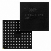
LPC3240FET296/01,5 NXP Semiconductors, LPC3240FET296/01,5 Datasheet - Page 3

LPC3240FET296/01,5
Manufacturer Part Number
LPC3240FET296/01,5
Description
IC ARM9 MCU 256K 296-TFBGA
Manufacturer
NXP Semiconductors
Series
LPC32x0r
Specifications of LPC3240FET296/01,5
Package / Case
296-TFBGA
Core Processor
ARM9
Core Size
16/32-Bit
Speed
266MHz
Connectivity
EBI/EMI, Ethernet, I²C, IrDA, Microwire, SPI, SSI, SSP, UART/USART, USB OTG
Peripherals
DMA, I²S, Motor Control PWM, PWM, WDT
Number Of I /o
51
Program Memory Type
ROMless
Ram Size
256K x 8
Voltage - Supply (vcc/vdd)
0.9 V ~ 3.6 V
Data Converters
A/D 3x10b
Oscillator Type
Internal
Operating Temperature
-40°C ~ 85°C
Processor Series
LPC32
Core
ARM926EJ-S
Data Bus Width
32 bit
Data Ram Size
256 KB
Interface Type
EMC
Maximum Clock Frequency
266 MHz
Number Of Timers
6
Operating Supply Voltage
1.31 V to 1.39 V
Maximum Operating Temperature
+ 85 C
Mounting Style
SMD/SMT
3rd Party Development Tools
MDK-ARM, RL-ARM, ULINK2
Minimum Operating Temperature
- 40 C
On-chip Adc
10 bit, 3 Channel
Lead Free Status / RoHS Status
Lead free / RoHS Compliant
Eeprom Size
-
Program Memory Size
-
Lead Free Status / Rohs Status
Lead free / RoHS Compliant
Other names
568-4963
935290765551
935290765551
Available stocks
Company
Part Number
Manufacturer
Quantity
Price
Company:
Part Number:
LPC3240FET296/01,5
Manufacturer:
NXP
Quantity:
630
Company:
Part Number:
LPC3240FET296/01,5
Manufacturer:
NXP Semiconductors
Quantity:
10 000
NXP Semiconductors
1. Product identification
2. Errata overview
Table 2.
ES_LPC3240
Errata sheet
Functional
problems
DMA.1
NOR.1
Ethernet.1
DDR.2
DDR.1
RTC.1
INT.1
MCPWM.1
HSUART.1
Functional problems table
Short description
Single burst DMA memory-to-memory transfers have
additional memory cycles when the DMA source
memory is on the EMC bus.
When booting from NOR flash, SDRAM devices will not
release the data bus, preventing the LPC3240 from
booting correctly
Ethernet TxConsumeIndex register does not update
correctly after the first frame is sent
DDR EMC_D[15:0] to EMC_DQS[1:0] data output
set-up time, t
limited timing margin
DDR interface has > 1.2 ns clock skew
An RTC match doesn't drive the ONSW pin active
(HIGH).
GPI_08 does not generate in interrupt signal.
Input pins (MCI0-2) on the Motor Control PWM
peripheral are not functional
High speed UART receive FIFO and status can freeze
The LPC3240 devices typically have the following top-side marking:
The last letter in the last line (field ‘R’) will identify the device revision. This Errata Sheet
covers the following revisions of the LPC3240:
Table 1.
[1]
[2]
Field ‘YY’ states the year the device was manufactured. Field ‘WW’ states the week the
device was manufactured during that year.
Revision identifier (R)
‘A’
‘-’
LPC3240FET296
xxxxxxx
xxYYWWR
[2]
[1]
Revision ‘A’ parts with and without the /01 suffix are identical. For example, LPC3240FET296 Revision ‘A’ is
identical to LPC3240FET296/01 Revision ‘A’.
Does not apply to /01 parts.
su(Q)
, for MCU write to DDR provides
Device revision table
All information provided in this document is subject to legal disclaimers.
Rev. 8 — 1 February 2011
Revision description
Second device revision
Initial device revision
Revision identifier
‘-’, ‘A’
‘-’, ‘A’
‘-’, ‘A’
‘-’, ‘A’
‘-’, ‘A’
‘-’, ‘A’
‘-’
‘-’, ‘A’
‘-’, ‘A’
ES_LPC3240
Errata sheet LPC3240
Detailed description
Section 3.1 on page 5
Section 3.2 on page 7
Section 3.3 on page 8
Section 3.4 on page 8
Section 3.5 on page 11
Section 3.6 on page 12
Section 3.7 on page 12
Section 3.8 on page 13
Section 3.9 on page 14
© NXP B.V. 2011. All rights reserved.
3 of 17


