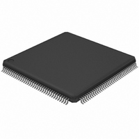
LPC2377FBD144,551 NXP Semiconductors, LPC2377FBD144,551 Datasheet - Page 15

LPC2377FBD144,551
Manufacturer Part Number
LPC2377FBD144,551
Description
IC ARM7 MCU FLASH 512K 144LQFP
Manufacturer
NXP Semiconductors
Series
LPC2300r
Datasheet
1.LPC2377FBD144551.pdf
(68 pages)
Specifications of LPC2377FBD144,551
Core Processor
ARM7
Core Size
16/32-Bit
Speed
72MHz
Connectivity
EBI/EMI, Ethernet, I²C, Microwire, SPI, SSI, SSP, UART/USART
Peripherals
Brown-out Detect/Reset, DMA, I²S, POR, PWM, WDT
Number Of I /o
104
Program Memory Size
512KB (512K x 8)
Program Memory Type
FLASH
Ram Size
58K x 8
Voltage - Supply (vcc/vdd)
3 V ~ 3.6 V
Data Converters
A/D 8x10b; D/A 1x10b
Oscillator Type
Internal
Operating Temperature
-40°C ~ 85°C
Package / Case
144-LQFP
Processor Series
LPC23
Core
ARM7TDMI-S
Data Bus Width
32 bit
Data Ram Size
58 KB
Interface Type
CAN, I2S, ISP, UART, USB
Maximum Clock Frequency
72 MHz
Number Of Programmable I/os
104
Number Of Timers
4
Operating Supply Voltage
3.3 V
Maximum Operating Temperature
+ 85 C
Mounting Style
SMD/SMT
3rd Party Development Tools
MDK-ARM, RL-ARM, ULINK2
Minimum Operating Temperature
- 40 C
On-chip Adc
10 bit, 8 Channel
On-chip Dac
10 bit, 1 Channel
Package
144LQFP
Device Core
ARM7TDMI-S
Family Name
LPC2000
Maximum Speed
72 MHz
For Use With
568-4310 - EVAL BOARD LPC2158 W/LCDMCB2370UME - BOARD EVAL MCB2370 + ULINK-MEMCB2370U - BOARD EVAL MCB2370 + ULINK2MCB2370 - BOARD EVAL NXP LPC2368/2378568-3999 - BOARD EVAL FOR LPC23 ARM MCU622-1005 - USB IN-CIRCUIT PROG ARM7 LPC2K
Lead Free Status / RoHS Status
Lead free / RoHS Compliant
Eeprom Size
-
Lead Free Status / Rohs Status
Details
Other names
568-4411
935286019551
LPC2377FBD144-S
935286019551
LPC2377FBD144-S
Available stocks
Company
Part Number
Manufacturer
Quantity
Price
Company:
Part Number:
LPC2377FBD144,551
Manufacturer:
NXP Semiconductors
Quantity:
10 000
NXP Semiconductors
Table 3.
[1]
[2]
[3]
[4]
[5]
[6]
[7]
[8]
[9]
[10] If the RTC is not used, these pins can be left floating.
[11] Pad provides special analog functionality.
[12] Pad provides special analog functionality.
[13] Pad provides special analog functionality.
[14] Pad provides special analog functionality.
[15] Pad provides special analog functionality.
[16] Pad provides special analog functionality.
LPC2377_78
Product data sheet
Symbol
V
n.c.
V
V
VREF
VBAT
DD(3V3)
DD(DCDC)(3V3)
DDA
5 V tolerant pad providing digital I/O functions with TTL levels and hysteresis.
5 V tolerant pad providing digital I/O functions (with TTL levels and hysteresis) and analog input. When configured as a DAC input,
digital section of the pad is disabled.
5 V tolerant pad providing digital I/O with TTL levels and hysteresis and analog output function. When configured as the DAC output,
digital section of the pad is disabled.
Open-drain, 5 V tolerant digital I/O pad compatible with I
functionality. When power is switched off, this pin connected to the I
configuration applies to all functions on this pin.
Pad provides digital I/O and USB functions (LPC2378 only). It is designed in accordance with the USB specification, revision 2.0
(Full-speed and Low-speed mode only).
5 V tolerant pad with 5 ns glitch filter providing digital I/O functions with TTL levels and hysteresis.
5 V tolerant pad with 20 ns glitch filter providing digital I/O function with TTL levels and hysteresis.
Pad provides special analog functionality.
When the main oscillator is not used, connect XTAL1 and XTAL2 as follows: XTAL1 can be left floating or can be grounded (grounding
is preferred to reduce susceptibility to noise). XTAL2 should be left floating.
Pin description
Pin
41, 62,
77, 102,
114,
138
21, 81,
98
18, 60,
121
14
17
27
[14]
[16]
[16]
[16]
[13]
[15]
…continued
Type
I
I
I
I
I
I
Description
3.3 V supply voltage: This is the power supply voltage for the I/O ports.
Leave these pins unconnected.
3.3 V DC-to-DC converter supply voltage: This is the power supply for the on-chip
DC-to-DC converter only.
analog 3.3 V pad supply voltage: This should be nominally the same voltage as
V
power the ADC and DAC.
ADC reference: This should be nominally the same voltage as V
be isolated to minimize noise and error. The level on this pin is used as a reference
for ADC and DAC.
RTC pin power supply: 3.3 V on this pin supplies the power to the RTC peripheral.
DD(3V3)
All information provided in this document is subject to legal disclaimers.
but should be isolated to minimize noise and error. This voltage is used to
Rev. 5 — 17 June 2010
2
C-bus 400 kHz specification. It requires an external pull-up to provide output
2
C-bus is floating and does not disturb the I
Single-chip 16-bit/32-bit microcontrollers
LPC2377/78
2
© NXP B.V. 2010. All rights reserved.
C lines. Open-drain
DD(3V3)
but should
15 of 68


