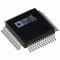
ADUC841BSZ62-5 Analog Devices Inc, ADUC841BSZ62-5 Datasheet - Page 34

ADUC841BSZ62-5
Manufacturer Part Number
ADUC841BSZ62-5
Description
IC ADC/DAC 12BIT W/MCU 52-MQFP
Manufacturer
Analog Devices Inc
Series
MicroConverter® ADuC8xxr
Datasheet
1.EVAL-ADUC842QS.pdf
(88 pages)
Specifications of ADUC841BSZ62-5
Core Size
8-Bit
Program Memory Size
62KB (62K x 8)
Core Processor
8052
Speed
20MHz
Connectivity
I²C, SPI, UART/USART
Peripherals
DMA, PSM, PWM, Temp Sensor, WDT
Number Of I /o
32
Program Memory Type
FLASH
Ram Size
2.25K x 8
Voltage - Supply (vcc/vdd)
4.75 V ~ 5.25 V
Data Converters
A/D 8x12b, D/A 2x12b
Oscillator Type
Internal
Operating Temperature
-40°C ~ 85°C
Package / Case
52-MQFP, 52-PQFP
Controller Family/series
(8051) 8052
No. Of I/o's
32
Ram Memory Size
2.25KB
Cpu Speed
20MIPS
No. Of Timers
3
No. Of Pwm Channels
2
Embedded Interface Type
UART
Rohs Compliant
Yes
Cpu Family
ADuC8xx
Device Core
8052
Device Core Size
8b
Frequency (max)
20MHz
Interface Type
I2C/SPI/UART
Total Internal Ram Size
2.25KB
# I/os (max)
34
Number Of Timers - General Purpose
3
Operating Supply Voltage (typ)
5V
Operating Supply Voltage (max)
5.25V
Operating Supply Voltage (min)
4.75V
On-chip Adc
8-chx12-bit
On-chip Dac
2-chx12-bit
Instruction Set Architecture
CISC
Operating Temp Range
-40C to 85C
Operating Temperature Classification
Industrial
Mounting
Surface Mount
Pin Count
52
Package Type
MQFP
Lead Free Status / RoHS Status
Lead free / RoHS Compliant
For Use With
EVAL-ADUC841QSZ - KIT DEV FOR ADUC841 QUICK START
Eeprom Size
-
Lead Free Status / Rohs Status
Compliant
Available stocks
Company
Part Number
Manufacturer
Quantity
Price
Company:
Part Number:
ADUC841BSZ62-5
Manufacturer:
Analog Devices Inc
Quantity:
135
Company:
Part Number:
ADUC841BSZ62-5
Manufacturer:
Analog Devices Inc
Quantity:
10 000
ADuC841/ADuC842/ADuC843
USING FLASH/EE DATA MEMORY
The 4 kBytes of Flash/EE data memory are configured as 1024
pages, each of 4 bytes. As with the other ADuC841/ADuC842/
ADuC843 peripherals, the interface to this memory space is via
a group of registers mapped in the SFR space. A group of four
data registers (EDATA1–4) is used to hold the four bytes of data
at each page. The page is addressed via the two registers, EADRH
and EADRL. Finally, ECON is an 8-bit control register that may
be written with one of nine Flash/EE memory access commands
to trigger various read, write, erase, and verify functions. A block
diagram of the SFR interface to the Flash/EE data memory array
is shown in Figure 41.
ECON—Flash/EE Memory Control SFR
Programming of either Flash/EE data memory or Flash/ EE
program memory is done through the Flash/EE memory
control SFR (ECON). This SFR allows the user to read, write,
erase, or verify the 4 kBytes of Flash/EE data memory or the
56 kBytes of Flash/EE program memory.
Table 12. ECON—Flash/EE Memory Commands
ECON VALUE
01H
READ
02H
WRITE
03H
04H
VERIFY
05H
ERASE PAGE
06H
ERASE ALL
81H
READBYTE
82H
WRITEBYTE
0FH
EXULOAD
F0H
ULOAD
Reserved.
Command Description (Normal Mode)
(Power-On Default)
Results in 4 bytes in the Flash/EE data memory, addressed
by the page address EADRH/L, being read into EDATA1–4.
Results in 4 bytes in EDATA1–4 being written to the
Flash/EE data memory at the page address given by
EADRH/L (0 – EADRH/L < 0400H).
Note that the 4 bytes in the page being addressed must
be pre-erased.
Verifies that the data in EDATA1–4 is contained in the
page address given by EADRH/L. A subsequent read of the
ECON SFR results in 0 being read if the verification is valid,
or a nonzero value being read to indicate an invalid
verification.
Results in erasing the 4-byte page of Flash/EE data
memory addressed by the page address EADRH/L.
Results in erasing the entire 4 kBytes of Flash/EE data
memory.
Results in the byte in the Flash/EE data memory,
addressed by the byte address EADRH/L, being read into
EDATA1 (0 – EADRH / L – 0FFFH).
Results in the byte in EDATA1 being written into Flash/EE
data memory at the byte address EADRH/L
Leaves the ECON instructions to operate on the Flash/EE
data memory.
Enters ULOAD mode, directing subsequent ECON
instructions to operate on the Flash/EE program memory.
Rev. 0 | Page 34 of 88
BYTE
ADDRESSES
ARE GIVEN IN
BRACKETS
3FEH
3FFH
03H
02H
01H
00H
Command Description (ULOAD Mode)
Not implemented. Use the MOVC instruction.
Results in bytes 0–255 of internal XRAM being written to
the 256 bytes of Flash/EE program memory at the page
address given by EADRH (0 – EADRH < E0H).
Note that the 256 bytes in the page being addressed must
be pre-erased.
Reserved.
Not implemented. Use the MOVC and MOVX instructions
to verify the write in software.
Results in the 64 byte page of Flash/EE program memory,
addressed by the byte address EADRH/L, being erased.
EADRL can equal any of 64 locations within the page. A
new page starts whenever EADRL is equal to 00H, 40H,
80H, or C0H.
Results in erasing the entire 56 kBytes of ULOAD Flash/EE
program memory.
Not implemented. Use the MOVC command.
Results in the byte in EDATA1 being written into Flash/EE
program memory at the byte address EADRH/L (0 –
EADRH/L – DFFFH).
Enters normal mode directing subsequent ECON
instructions to operate on the Flash/EE data memory.
Leaves the ECON instructions to operate on the Flash/EE
program memory.
Figure 41. Flash/EE Data Memory Control and Configuration
(0FFCH)
(0FF8H)
(000CH)
(0004H)
(0000H)
(0008H)
BYTE 1
BYTE 1
BYTE 1
BYTE 1
BYTE 1
BYTE 1
(000DH)
(0FFDH)
(0FF9H)
(0009H)
(0005H)
(0001H)
BYTE 2
BYTE 2
BYTE 2
BYTE 2
BYTE 2
BYTE 2
(0FFEH)
(0FFAH)
(000AH)
(000EH)
(0002H)
BYTE 3
(0006H)
BYTE 3
BYTE 3
BYTE 3
BYTE 3
BYTE 3
(0FFBH)
(0FFFH)
(000FH)
(000BH)
(0007H)
(0003H)
BYTE 4
BYTE 4
BYTE 4
BYTE 4
BYTE 4
BYTE 4


