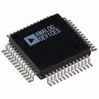
ADUC841BSZ62-5 Analog Devices Inc, ADUC841BSZ62-5 Datasheet - Page 4

ADUC841BSZ62-5
Manufacturer Part Number
ADUC841BSZ62-5
Description
IC ADC/DAC 12BIT W/MCU 52-MQFP
Manufacturer
Analog Devices Inc
Series
MicroConverter® ADuC8xxr
Datasheet
1.EVAL-ADUC842QS.pdf
(88 pages)
Specifications of ADUC841BSZ62-5
Core Size
8-Bit
Program Memory Size
62KB (62K x 8)
Core Processor
8052
Speed
20MHz
Connectivity
I²C, SPI, UART/USART
Peripherals
DMA, PSM, PWM, Temp Sensor, WDT
Number Of I /o
32
Program Memory Type
FLASH
Ram Size
2.25K x 8
Voltage - Supply (vcc/vdd)
4.75 V ~ 5.25 V
Data Converters
A/D 8x12b, D/A 2x12b
Oscillator Type
Internal
Operating Temperature
-40°C ~ 85°C
Package / Case
52-MQFP, 52-PQFP
Controller Family/series
(8051) 8052
No. Of I/o's
32
Ram Memory Size
2.25KB
Cpu Speed
20MIPS
No. Of Timers
3
No. Of Pwm Channels
2
Embedded Interface Type
UART
Rohs Compliant
Yes
Cpu Family
ADuC8xx
Device Core
8052
Device Core Size
8b
Frequency (max)
20MHz
Interface Type
I2C/SPI/UART
Total Internal Ram Size
2.25KB
# I/os (max)
34
Number Of Timers - General Purpose
3
Operating Supply Voltage (typ)
5V
Operating Supply Voltage (max)
5.25V
Operating Supply Voltage (min)
4.75V
On-chip Adc
8-chx12-bit
On-chip Dac
2-chx12-bit
Instruction Set Architecture
CISC
Operating Temp Range
-40C to 85C
Operating Temperature Classification
Industrial
Mounting
Surface Mount
Pin Count
52
Package Type
MQFP
Lead Free Status / RoHS Status
Lead free / RoHS Compliant
For Use With
EVAL-ADUC841QSZ - KIT DEV FOR ADUC841 QUICK START
Eeprom Size
-
Lead Free Status / Rohs Status
Compliant
Available stocks
Company
Part Number
Manufacturer
Quantity
Price
Company:
Part Number:
ADUC841BSZ62-5
Manufacturer:
Analog Devices Inc
Quantity:
135
Company:
Part Number:
ADUC841BSZ62-5
Manufacturer:
Analog Devices Inc
Quantity:
10 000
ADuC841/ADuC842/ADuC843
Parameter
DAC AC CHARACTERISTICS
DAC CHANNEL SPECIFICATIONS
Internal Buffer Disabled ADuC841/ADuC842 Only
DC ACCURACY
ANALOG OUTPUTS
REFERENCE INPUT/OUTPUT REFERENCE OUTPUT
EXTERNAL REFERENCE INPUT
POWER SUPPLY MONITOR (PSM)
WATCHDOG TIMER (WDT)
FLASH/EE MEMORY RELIABILITY CHARACTERISTICS
DIGITAL INPUTS
RESET
Voltage Output Settling Time
Digital-to-Analog Glitch Energy
Resolution
Relative Accuracy
Differential Nonlinearity
Offset Error
Gain Error
Gain Error Mismatch
Voltage Range_0
Output Voltage (V
Accuracy
Power Supply Rejection
Reference Temperature Coefficient
Internal V
Voltage Range (V
Input Impedance
Input Leakage
DV
DV
Timeout Period
Endurance
Data Retention
Input Leakage Current (Port 0, EA )
Logic 1 Input Current
(All Digital Inputs), SDATA, SCLOCK
Logic 0 Input Current (Ports 1, 2, 3) SDATA, SCLOCK
Logic 1 to Logic 0 Transition Current (Ports 2 and 3)
DD
DD
Trip Point Selection Range
Power Supply Trip Point Accuracy
REF
17
10
Power-On Time
18
REF
REF
)
)
4
4
4
11
15
12, 13
14
16
V
15
10
12
±3
–1
±1/2
±5
±0.5
0.5
0 to V
2.5
±10
65
±15
2
1
V
20
1
0
2000
100,000
100
±10
±1
±10
±1
–75
–40
–660
–400
±10
10
105
Rev. 0 | Page 4 of 88
DD
DD
= 5 V
REF
V
15
10
12
±3
–1
±1/2
±5
±0.5
0.5
0 to V
2.5
±10
67
±15
2
1
V
20
1
2.93
3.08
±2.5
0
2000
100,000
100
±10
±1
±10
±1
–25
–15
–250
–140
±10
5
35
DD
DD
= 3 V
REF
Unit
µs typ
nV-sec typ
Bits
LSB typ
LSB max
LSB typ
mV max
% typ
% typ
V typ
V
mV Max
dB typ
ppm/°C typ
ms typ
V min
V max
kΩ typ
µA max
V min
V max
% max
ms min
ms max
Cycles min
Years min
µA max
µA typ
µA max
µA typ
µA max
µA typ
µA max
µA typ
µA max
µA min
µA max
Test Conditions/Comments
Full-scale settling time to within
½ LSB of final value
1 LSB change at major carry
Guaranteed 12-bit monotonic
V
V
% of full-scale on DAC1
DAC V
Of V
T
Internal band gap deselected via
ADCCON1.6
Two trip points selectable in this
range programmed via TPD1–0 in
PSMCON, 3 V part only
Nine timeout periods selectable in
this range
V
V
V
V
V
V
V
V
V
V
REF
REF
A
IN
IN
IN
IN
IL
IL
IL
IN
IN
IN
= 25°C
= 450 mV
= 2 V
= 2 V
= 0 V or V
= 0 V or V
= V
= V
= 0 V
= 5 V, 3 V Internal Pull Down
= 5 V, 3 V Internal Pull Down
range
range
REF
REF
DD
DD
measured at the C
= 2.5 V
DD
DD
REF
pin


