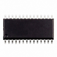
ST72F264G1M6 STMicroelectronics, ST72F264G1M6 Datasheet - Page 78

ST72F264G1M6
Manufacturer Part Number
ST72F264G1M6
Description
IC MCU 8BIT 4K 28 SOIC
Manufacturer
STMicroelectronics
Series
ST7r
Datasheet
1.STEVAL-ISQ002V1.pdf
(172 pages)
Specifications of ST72F264G1M6
Core Processor
ST7
Core Size
8-Bit
Speed
16MHz
Connectivity
I²C, SCI, SPI
Peripherals
LVD, POR, PWM, WDT
Number Of I /o
22
Program Memory Size
4KB (4K x 8)
Program Memory Type
FLASH
Ram Size
256 x 8
Voltage - Supply (vcc/vdd)
2.7 V ~ 5.5 V
Data Converters
A/D 6x10b
Oscillator Type
Internal
Operating Temperature
-40°C ~ 85°C
Package / Case
28-SOIC (7.5mm Width)
Processor Series
ST72F2x
Core
ST7
Data Bus Width
8 bit
Data Ram Size
256 B
Interface Type
I2C, SCI, SPI
Maximum Clock Frequency
8 MHz
Number Of Programmable I/os
22
Number Of Timers
4 bit
Operating Supply Voltage
2.7 V to 5.5 V
Maximum Operating Temperature
+ 85 C
Mounting Style
SMD/SMT
Development Tools By Supplier
ST7F264-IND/USB, ST72F34X-SK/RAIS, ST7MDT10-DVP3, ST7MDT10-EMU3, STX-RLINK
Minimum Operating Temperature
- 40 C
On-chip Adc
16 bit
For Use With
497-6423 - BOARD EVAL BASED ON ST72264G1497-5046 - KIT TOOL FOR ST7/UPSD/STR7 MCU
Lead Free Status / RoHS Status
Request inventory verification / Request inventory verification
Eeprom Size
-
Lead Free Status / Rohs Status
Details
Other names
497-2105-5
Available stocks
Company
Part Number
Manufacturer
Quantity
Price
ST72260Gx, ST72262Gx, ST72264Gx
SERIAL PERIPHERAL INTERFACE (Cont’d)
11.4.3.2 Slave Select Management
As an alternative to using the SS pin to control the
Slave Select signal, the application can choose to
manage the Slave Select signal by software. This
is configured by the SSM bit in the SPICSR regis-
ter (see
In software management, the external SS pin is
free for other application uses and the internal SS
signal level is driven by writing to the SSI bit in the
SPICSR register.
In Master mode:
Figure 48. Generic SS Timing Diagram
Figure 49. Hardware/Software Slave Select Management
78/172
– SS internal must be held high continuously
MOSI/MISO
(if CPHA=0)
(if CPHA=1)
Figure
Master SS
Slave SS
Slave SS
49)
SS external pin
SSI bit
Byte 1
SSM bit
1
0
SS internal
In Slave Mode:
There are two cases depending on the data/clock
timing relationship (see
If CPHA=1 (data latched on 2nd clock edge):
If CPHA=0 (data latched on 1st clock edge):
Byte 2
– SS internal must be held low during the entire
– SS internal must be held low during byte
transmission. This implies that in single slave
applications the SS pin either can be tied to
V
ing the SS function by software (SSM= 1 and
SSI=0 in the in the SPICSR register)
transmission and pulled high between each
byte to allow the slave to write to the shift reg-
ister. If SS is not pulled high, a Write Collision
error will occur when the slave writes to the
shift register (see
SS
, or made free for standard I/O by manag-
Byte 3
Section
Figure
11.4.5.3).
48):


