DSP56F801FA80E Freescale Semiconductor, DSP56F801FA80E Datasheet - Page 10
DSP56F801FA80E
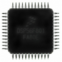
Manufacturer Part Number
DSP56F801FA80E
Description
IC DSP 80MHZ 8K FLASH 48-LQFP
Manufacturer
Freescale Semiconductor
Series
56F8xxr
Datasheet
1.DSP56F801EVM.pdf
(48 pages)
Specifications of DSP56F801FA80E
Core Processor
56800
Core Size
16-Bit
Speed
80MHz
Connectivity
SCI, SPI
Peripherals
POR, PWM, WDT
Number Of I /o
11
Program Memory Size
20KB (10K x 16)
Program Memory Type
FLASH
Ram Size
2K x 16
Voltage - Supply (vcc/vdd)
3 V ~ 3.6 V
Data Converters
A/D 8x12b
Oscillator Type
Internal
Operating Temperature
-40°C ~ 85°C
Package / Case
48-LQFP
Package
48LQFP
Family Name
56F8xx
Maximum Speed
80 MHz
Operating Supply Voltage
3.3 V
Data Bus Width
16 Bit
Number Of Programmable I/os
11
Interface Type
SCI/SPI
On-chip Adc
2(4-chx12-bit)
Number Of Timers
1
Lead Free Status / RoHS Status
Lead free / RoHS Compliant
Eeprom Size
-
Available stocks
Company
Part Number
Manufacturer
Quantity
Price
Company:

Part Number:
DSP56F801FA80E
Manufacturer:
Freescale Semiconductor
Quantity:
10 000
Part Number:
DSP56F801FA80E
Manufacturer:
FREESCALE
Quantity:
20 000


2.2 Power and Ground Signals
2.3 Clock and Phase Locked Loop Signals
10
No. of
No. of
Pins
No. of Pins
Pins
No. of Pins
2
1
4
1
1
4
1
GPIOB2
VCAPC
EXTAL
Signal
Signal
Name
Name
Signal Name
Signal Name
Supply
V
Signal
TCS
Signal
Output
V
V
Type
Input/
Type
Input
V
SSA
DDA
SS
DD
During Reset
During Reset
Power—These pins provide power to the internal structures of the chip, and should all be
attached to V
Analog Power—This pin is a dedicated power pin for the analog portion of the chip and
should be connected to a low noise 3.3V supply.
GND—These pins provide grounding for the internal structures of the chip, and should all
be attached to V
Analog Ground—This pin supplies an analog ground.
TCS—This Schmitt pin is reserved for factory use and must be tied to V
In block diagrams, this pin is considered an additional V
Table 2-4 Supply Capacitors and VPP
Supply
State
State
Input
Input
Table 2-5 PLL and Clock
56F801 Technical Data, Rev. 17
Table 2-2 Power Inputs
DD.
External Crystal Oscillator Input—This input should be connected to an
8MHz external crystal or ceramic resonator. For more information, please
refer to
Port B GPIO—This multiplexed pin is a General Purpose I/O (GPIO) pin that
can be programmed as an input or output pin. This I/O can be utilized when
using the on-chip relaxation oscillator so the EXTAL pin is not needed.
Table 2-3 Grounds
VCAPC—Connect each pin to a 2.2 μFor greater bypass capacitor in order
to bypass the core logic voltage regulator (required for proper chip
operation). For more information, refer to
SS.
Section
3.5.
Signal Description
Signal Description
Signal Description
Signal Description
SS.
Section
5.2.
Freescale Semiconductor
SS
for normal use.
Related parts for DSP56F801FA80E
Image
Part Number
Description
Manufacturer
Datasheet
Request
R

Part Number:
Description:
KIT LEARNING DSP 16BIT CSM56F801
Manufacturer:
Freescale Semiconductor
Datasheet:

Part Number:
Description:
Manufacturer:
Freescale Semiconductor, Inc
Datasheet:
Part Number:
Description:
Manufacturer:
Freescale Semiconductor, Inc
Datasheet:
Part Number:
Description:
Manufacturer:
Freescale Semiconductor, Inc
Datasheet:
Part Number:
Description:
Manufacturer:
Freescale Semiconductor, Inc
Datasheet:
Part Number:
Description:
Manufacturer:
Freescale Semiconductor, Inc
Datasheet:
Part Number:
Description:
Manufacturer:
Freescale Semiconductor, Inc
Datasheet:
Part Number:
Description:
Manufacturer:
Freescale Semiconductor, Inc
Datasheet:
Part Number:
Description:
Manufacturer:
Freescale Semiconductor, Inc
Datasheet:
Part Number:
Description:
Manufacturer:
Freescale Semiconductor, Inc
Datasheet:
Part Number:
Description:
Manufacturer:
Freescale Semiconductor, Inc
Datasheet:
Part Number:
Description:
Manufacturer:
Freescale Semiconductor, Inc
Datasheet:
Part Number:
Description:
Manufacturer:
Freescale Semiconductor, Inc
Datasheet:
Part Number:
Description:
Manufacturer:
Freescale Semiconductor, Inc
Datasheet:
Part Number:
Description:
Manufacturer:
Freescale Semiconductor, Inc
Datasheet: