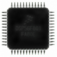
DSP56F801FA80E Freescale Semiconductor, DSP56F801FA80E Datasheet - Page 45

DSP56F801FA80E
Manufacturer Part Number
DSP56F801FA80E
Description
IC DSP 80MHZ 8K FLASH 48-LQFP
Manufacturer
Freescale Semiconductor
Series
56F8xxr
Datasheet
1.DSP56F801EVM.pdf
(48 pages)
Specifications of DSP56F801FA80E
Core Processor
56800
Core Size
16-Bit
Speed
80MHz
Connectivity
SCI, SPI
Peripherals
POR, PWM, WDT
Number Of I /o
11
Program Memory Size
20KB (10K x 16)
Program Memory Type
FLASH
Ram Size
2K x 16
Voltage - Supply (vcc/vdd)
3 V ~ 3.6 V
Data Converters
A/D 8x12b
Oscillator Type
Internal
Operating Temperature
-40°C ~ 85°C
Package / Case
48-LQFP
Package
48LQFP
Family Name
56F8xx
Maximum Speed
80 MHz
Operating Supply Voltage
3.3 V
Data Bus Width
16 Bit
Number Of Programmable I/os
11
Interface Type
SCI/SPI
On-chip Adc
2(4-chx12-bit)
Number Of Timers
1
Lead Free Status / RoHS Status
Lead free / RoHS Compliant
Eeprom Size
-
Available stocks
Company
Part Number
Manufacturer
Quantity
Price
Company:
Part Number:
DSP56F801FA80E
Manufacturer:
Freescale Semiconductor
Quantity:
10 000
Part Number:
DSP56F801FA80E
Manufacturer:
FREESCALE
Quantity:
20 000
Freescale Semiconductor
•
•
•
•
•
•
Bypass the V
capacitor such as a tantalum capacitor.
Because the controller’s output signals have fast rise and fall times, PCB trace lengths should be minimal.
Consider all device loads as well as parasitic capacitance due to PCB traces when calculating capacitance.
This is especially critical in systems with higher capacitive loads that could create higher transient currents
in the V
Take special care to minimize noise levels on the VREF, V
Designs that utilize the TRST pin for JTAG port or OnCE module functionality (such as development or
debugging systems) should allow a means to assert TRST whenever RESET is asserted, as well as a means
to assert TRST independently of RESET. TRST must be asserted at power up for proper operation. Designs
that do not require debugging functionality, such as consumer products, TRST should be tied low.
Because the Flash memory is programmed through the JTAG/OnCE port, designers should provide an
interface to this port to allow in-circuit Flash programming.
DD
and GND circuits.
DD
and V
SS
layers of the PCB with approximately 100 μF, preferably with a high-grade
56F801 Technical Data, Rev. 17
DDA
and V
SSA
pins.
Electrical Design Considerations
45


