MC908GP32CPE Freescale Semiconductor, MC908GP32CPE Datasheet - Page 72
MC908GP32CPE
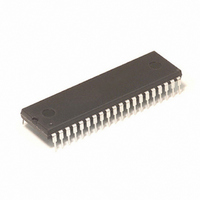
Manufacturer Part Number
MC908GP32CPE
Description
IC MCU 8MHZ 32K FLASH 40-DIP
Manufacturer
Freescale Semiconductor
Series
HC08r
Datasheet
1.MC908GP32CFBE.pdf
(266 pages)
Specifications of MC908GP32CPE
Core Processor
HC08
Core Size
8-Bit
Speed
8MHz
Connectivity
SCI, SPI
Peripherals
LVD, POR, PWM
Number Of I /o
33
Program Memory Size
32KB (32K x 8)
Program Memory Type
FLASH
Ram Size
512 x 8
Voltage - Supply (vcc/vdd)
2.7 V ~ 5.5 V
Data Converters
A/D 8x8b
Oscillator Type
Internal
Operating Temperature
-40°C ~ 85°C
Package / Case
40-DIP (0.600", 15.24mm)
Processor Series
HC08GP
Core
HC08
Data Bus Width
8 bit
Data Ram Size
512 B
Interface Type
SCI, SPI
Maximum Clock Frequency
8 MHz
Number Of Programmable I/os
33
Number Of Timers
4
Maximum Operating Temperature
+ 85 C
Mounting Style
Through Hole
Development Tools By Supplier
FSICEBASE, DEMO908GZ60E, M68CBL05CE, M68EML08GPGTE
Minimum Operating Temperature
- 40 C
On-chip Adc
8 bit, 8 Channel
Lead Free Status / RoHS Status
Lead free / RoHS Compliant
Eeprom Size
-
Lead Free Status / Rohs Status
Details
Available stocks
Company
Part Number
Manufacturer
Quantity
Price
Company:

Part Number:
MC908GP32CPE
Manufacturer:
NXP
Quantity:
9 282
Part Number:
MC908GP32CPE
Manufacturer:
FREESCALE
Quantity:
20 000


Clock Generator Module (CGM)
5.5.1 PLL Control Register
The PLL control register (PCTL) contains the interrupt enable and flag bits, the on/off switch, the base
clock selector bit, the prescaler bits, and the VCO power-of-two range selector bits.
PLLIE — PLL Interrupt Enable Bit
PLLF — PLL Interrupt Flag Bit
PLLON — PLL On Bit
BCS — Base Clock Select Bit
72
This read/write bit enables the PLL to generate an interrupt request when the LOCK bit toggles, setting
the PLL flag, PLLF. When the AUTO bit in the PLL bandwidth control register (PBWC) is clear, PLLIE
cannot be written and reads as logic 0. Reset clears the PLLIE bit.
This read-only bit is set whenever the LOCK bit toggles. PLLF generates an interrupt request if the
PLLIE bit also is set. PLLF always reads as logic 0 when the AUTO bit in the PLL bandwidth control
register (PBWC) is clear. Clear the PLLF bit by reading the PLL control register. Reset clears the PLLF
bit.
This read/write bit activates the PLL and enables the VCO clock, CGMVCLK. PLLON cannot be
cleared if the VCO clock is driving the base clock, CGMOUT (BCS = 1). (See
Selector
This read/write bit selects either the crystal oscillator output, CGMXCLK, or the VCO clock,
CGMVCLK, as the source of the CGM output, CGMOUT. CGMOUT frequency is one-half the
frequency of the selected clock. BCS cannot be set while the PLLON bit is clear. After toggling BCS,
it may take up to three CGMXCLK and three CGMVCLK cycles to complete the transition from one
source clock to the other. During the transition, CGMOUT is held in stasis. (See
Selector
1 = PLL interrupts enabled
0 = PLL interrupts disabled
1 = Change in lock condition
0 = No change in lock condition
1 = PLL on
0 = PLL off
1 = CGMVCLK divided by two drives CGMOUT
0 = CGMXCLK divided by two drives CGMOUT
Circuit.) Reset sets this bit so that the loop can stabilize as the MCU is powering up.
Circuit.) Reset clears the BCS bit.
Address:
Do not inadvertently clear the PLLF bit. Any read or read-modify-write
operation on the PLL control register clears the PLLF bit.
PLLON and BCS have built-in protection that prevents the base clock
selector circuit from selecting the VCO clock as the source of the base clock
Reset:
Read:
Write:
$0036
PLLIE
Bit 7
0
= Unimplemented
Figure 5-4. PLL Control Register (PCTL)
PLLF
6
0
MC68HC908GP32 Data Sheet, Rev. 10
PLLON
5
1
NOTE
NOTE
BCS
4
0
PRE1
3
0
PRE0
2
0
VPR1
1
0
5.3.8 Base Clock
Freescale Semiconductor
5.3.8 Base Clock
VPR0
Bit 0
0
Related parts for MC908GP32CPE
Image
Part Number
Description
Manufacturer
Datasheet
Request
R

Part Number:
Description:
Manufacturer:
Freescale Semiconductor, Inc
Datasheet:
Part Number:
Description:
Manufacturer:
Freescale Semiconductor, Inc
Datasheet:
Part Number:
Description:
Manufacturer:
Freescale Semiconductor, Inc
Datasheet:
Part Number:
Description:
Manufacturer:
Freescale Semiconductor, Inc
Datasheet:
Part Number:
Description:
Manufacturer:
Freescale Semiconductor, Inc
Datasheet:
Part Number:
Description:
Manufacturer:
Freescale Semiconductor, Inc
Datasheet:
Part Number:
Description:
Manufacturer:
Freescale Semiconductor, Inc
Datasheet:
Part Number:
Description:
Manufacturer:
Freescale Semiconductor, Inc
Datasheet:
Part Number:
Description:
Manufacturer:
Freescale Semiconductor, Inc
Datasheet:
Part Number:
Description:
Manufacturer:
Freescale Semiconductor, Inc
Datasheet:
Part Number:
Description:
Manufacturer:
Freescale Semiconductor, Inc
Datasheet:
Part Number:
Description:
Manufacturer:
Freescale Semiconductor, Inc
Datasheet:
Part Number:
Description:
Manufacturer:
Freescale Semiconductor, Inc
Datasheet:
Part Number:
Description:
Manufacturer:
Freescale Semiconductor, Inc
Datasheet:
Part Number:
Description:
Manufacturer:
Freescale Semiconductor, Inc
Datasheet: