MC56F8367VPYE Freescale Semiconductor, MC56F8367VPYE Datasheet - Page 112
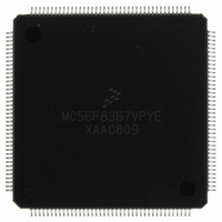
MC56F8367VPYE
Manufacturer Part Number
MC56F8367VPYE
Description
IC DSP 16BIT 60MHZ 160-LQFP
Manufacturer
Freescale Semiconductor
Series
56F8xxxr
Specifications of MC56F8367VPYE
Core Processor
56800
Core Size
16-Bit
Speed
60MHz
Connectivity
CAN, EBI/EMI, SCI, SPI
Peripherals
POR, PWM, Temp Sensor, WDT
Number Of I /o
76
Program Memory Size
544KB (272K x 16)
Program Memory Type
FLASH
Ram Size
18K x 16
Voltage - Supply (vcc/vdd)
2.25 V ~ 3.6 V
Data Converters
A/D 16x12b
Oscillator Type
External
Operating Temperature
-40°C ~ 105°C
Package / Case
160-LQFP
Cpu Family
56F8xxx
Device Core Size
16b
Frequency (max)
60MHz
Interface Type
CAN/SCI/SPI
Total Internal Ram Size
36KB
# I/os (max)
76
Number Of Timers - General Purpose
4
Operating Supply Voltage (typ)
3.3V
Operating Supply Voltage (max)
3.6V
Operating Supply Voltage (min)
3V
On-chip Adc
4(4-chx12-bit)
Instruction Set Architecture
CISC
Operating Temp Range
-40C to 105C
Operating Temperature Classification
Industrial
Mounting
Surface Mount
Pin Count
160
Package Type
LQFP
Data Bus Width
16 bit
Processor Series
MC56F83xx
Core
56800E
Numeric And Arithmetic Format
Fixed-Point
Device Million Instructions Per Second
60 MIPs
Maximum Clock Frequency
60 MHz
Number Of Programmable I/os
76
Data Ram Size
36 KB
Operating Supply Voltage
3.3 V
Maximum Operating Temperature
+ 105 C
Mounting Style
SMD/SMT
Development Tools By Supplier
MC56F8367EVME
Minimum Operating Temperature
- 40 C
Package
160LQFP
Family Name
56F8xxx
Maximum Speed
60 MHz
Number Of Timers
4
For Use With
MC56F8367EVME - EVAL BOARD FOR MC56F83X
Lead Free Status / RoHS Status
Lead free / RoHS Compliant
Eeprom Size
-
Lead Free Status / Rohs Status
Compliant
Available stocks
Company
Part Number
Manufacturer
Quantity
Price
Company:

Part Number:
MC56F8367VPYE
Manufacturer:
AM
Quantity:
90
Company:
Part Number:
MC56F8367VPYE
Manufacturer:
Freescale Semiconductor
Quantity:
10 000
Part Number:
MC56F8367VPYE
Manufacturer:
FREESCALE
Quantity:
20 000


6.3 Operating Modes
Since the SIM is responsible for distributing clocks and resets across the chip, it must understand the
various chip operating modes and take appropriate action. These are:
6.4 Operating Mode Register
The reset state for MB and MA will depend on the Flash secured state. See
information on how the Operating Mode Register (OMR) MA and MB bits operate in this device. For all
other bits, see the DSP56800E Reference Manual.
Note:
112
•
•
•
•
•
RESET
Type
Bit
Reset Mode, which has two submodes:
— POR and RESET operation
— COP reset and software reset operation
Run Mode
This is the primary mode of operation for this device. In this mode, the 56800E controls chip operation
Debug Mode
The 56800E is controlled via JTAG/EOnCE when in debug mode. All peripherals, except the COP and
PWMs, continue to run. COP is disabled and PWM outputs are optionally switched off to disable any motor
from being driven; see the PWM chapter in the 56F8300 Peripheral User Manual for details.
Wait Mode
In Wait mode, the core clock and memory clocks are disabled. Optionally, the COP can be stopped.
Similarly, it is an option to switch off PWM outputs to disable any motor from being driven. All other
peripherals continue to run.
Stop Mode
When in Stop mode, the 56800E core, memory, and most peripheral clocks are shut down. Optionally, the
COP and CAN can be stopped. For lowest power consumption in Stop mode, the PLL can be shut down.
This must be done explicitly before entering Stop mode, since there is no automatic mechanism for this. The
CAN (along with any non-gated interrupt) is capable of waking the chip up from Stop mode, but is not fully
functional in Stop mode.
The 56800E core and all peripherals are reset. This occurs when the internal POR is asserted or the
RESET pin is asserted.
The 56800E core and all peripherals are reset. The MA bit within the OMR is not changed. This allows
the software to determine the boot mode (internal or external boot) to be used on the next reset.
The OMR is not a Memory Map register; it is directly accessible in code through the acronym OMR.
R/W
15
NL
0
14
0
13
0
12
0
11
0
56F8367 Technical Data, Rev. 8
10
Figure 6-1 OMR
0
9
0
R/W
CM
8
0
R/W
XP
7
0
R/W
SD
6
0
R/W
5
R
0
Part 4.2
R/W
SA
4
0
R/W
EX
3
0
and
Freescale Semiconductor
Part 7
2
0
0
R/W
MB
1
X
for detailed
Preliminary
R/W
MA
X
0
Related parts for MC56F8367VPYE
Image
Part Number
Description
Manufacturer
Datasheet
Request
R

Part Number:
Description:
56f8300 16-bit Digital Signal Controllers
Manufacturer:
Freescale Semiconductor, Inc
Datasheet:
Part Number:
Description:
Manufacturer:
Freescale Semiconductor, Inc
Datasheet:
Part Number:
Description:
Manufacturer:
Freescale Semiconductor, Inc
Datasheet:
Part Number:
Description:
Manufacturer:
Freescale Semiconductor, Inc
Datasheet:
Part Number:
Description:
Manufacturer:
Freescale Semiconductor, Inc
Datasheet:
Part Number:
Description:
Manufacturer:
Freescale Semiconductor, Inc
Datasheet:
Part Number:
Description:
Manufacturer:
Freescale Semiconductor, Inc
Datasheet:
Part Number:
Description:
Manufacturer:
Freescale Semiconductor, Inc
Datasheet:
Part Number:
Description:
Manufacturer:
Freescale Semiconductor, Inc
Datasheet:
Part Number:
Description:
Manufacturer:
Freescale Semiconductor, Inc
Datasheet:
Part Number:
Description:
Manufacturer:
Freescale Semiconductor, Inc
Datasheet:
Part Number:
Description:
Manufacturer:
Freescale Semiconductor, Inc
Datasheet:
Part Number:
Description:
Manufacturer:
Freescale Semiconductor, Inc
Datasheet:
Part Number:
Description:
Manufacturer:
Freescale Semiconductor, Inc
Datasheet:
Part Number:
Description:
Manufacturer:
Freescale Semiconductor, Inc
Datasheet: