MC56F8367VPYE Freescale Semiconductor, MC56F8367VPYE Datasheet - Page 123
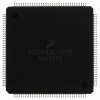
MC56F8367VPYE
Manufacturer Part Number
MC56F8367VPYE
Description
IC DSP 16BIT 60MHZ 160-LQFP
Manufacturer
Freescale Semiconductor
Series
56F8xxxr
Specifications of MC56F8367VPYE
Core Processor
56800
Core Size
16-Bit
Speed
60MHz
Connectivity
CAN, EBI/EMI, SCI, SPI
Peripherals
POR, PWM, Temp Sensor, WDT
Number Of I /o
76
Program Memory Size
544KB (272K x 16)
Program Memory Type
FLASH
Ram Size
18K x 16
Voltage - Supply (vcc/vdd)
2.25 V ~ 3.6 V
Data Converters
A/D 16x12b
Oscillator Type
External
Operating Temperature
-40°C ~ 105°C
Package / Case
160-LQFP
Cpu Family
56F8xxx
Device Core Size
16b
Frequency (max)
60MHz
Interface Type
CAN/SCI/SPI
Total Internal Ram Size
36KB
# I/os (max)
76
Number Of Timers - General Purpose
4
Operating Supply Voltage (typ)
3.3V
Operating Supply Voltage (max)
3.6V
Operating Supply Voltage (min)
3V
On-chip Adc
4(4-chx12-bit)
Instruction Set Architecture
CISC
Operating Temp Range
-40C to 105C
Operating Temperature Classification
Industrial
Mounting
Surface Mount
Pin Count
160
Package Type
LQFP
Data Bus Width
16 bit
Processor Series
MC56F83xx
Core
56800E
Numeric And Arithmetic Format
Fixed-Point
Device Million Instructions Per Second
60 MIPs
Maximum Clock Frequency
60 MHz
Number Of Programmable I/os
76
Data Ram Size
36 KB
Operating Supply Voltage
3.3 V
Maximum Operating Temperature
+ 105 C
Mounting Style
SMD/SMT
Development Tools By Supplier
MC56F8367EVME
Minimum Operating Temperature
- 40 C
Package
160LQFP
Family Name
56F8xxx
Maximum Speed
60 MHz
Number Of Timers
4
For Use With
MC56F8367EVME - EVAL BOARD FOR MC56F83X
Lead Free Status / RoHS Status
Lead free / RoHS Compliant
Eeprom Size
-
Lead Free Status / Rohs Status
Compliant
Available stocks
Company
Part Number
Manufacturer
Quantity
Price
Company:

Part Number:
MC56F8367VPYE
Manufacturer:
AM
Quantity:
90
Company:
Part Number:
MC56F8367VPYE
Manufacturer:
Freescale Semiconductor
Quantity:
10 000
Part Number:
MC56F8367VPYE
Manufacturer:
FREESCALE
Quantity:
20 000


6.5.8.2
This bit selects the alternate function for GPIOD1.
6.5.8.3
6.5.8.4
This bit selects the alternate function for GPIOC3.
6.5.8.5
This bit selects the alternate function for GPIOC2.
6.5.8.6
This bit selects the alternate function for GPIOC1.
6.5.8.7
This bit selects the alternate function for GPIOC0.
6.5.9
The Peripheral Clock Enable register is used enable or disable clocks to the peripherals as a power savings
feature. The clocks can be individually controlled for each peripheral on the chip.
Freescale Semiconductor
Preliminary
•
•
•
•
•
•
•
•
•
•
•
•
Base + $C
RESET
Read
Write
0 = CS3
1 = CAN2_RX
0 = CS2
1 = CAN2_TX
0 = HOME1/TB3 (default - see “Switch Matrix Mode” bits of the Quad Decoder DECCR register in the
56F8300 Peripheral User Manual)
1 = SS1
0 = INDEX1/TB2 (default)
1 = MISO1
0 = PHASEB1/TB1 (default)
1 = MOSI1
0 = PHASEA1/TB0 (default)
1 = SCLK1
Peripheral Clock Enable Register (SIM_PCE)
GPIOD1 (D1)—Bit 5
GPIOD0 (D0)—Bit 4
GPIOC3 (C3)—Bit 3
GPIOC2 (C2)—Bit 2
GPIOC1 (C1)—Bit 1
GPIOC0 (C0)—Bit 0
EMI
15
1
Figure 6-13 Peripheral Clock Enable Register (SIM_PCE)
ADCB ADCA CAN DEC1 DEC0 TMRD TMRC
14
1
13
1
12
1
11
1
56F8367 Technical Data, Rev. 8
10
1
9
1
8
1
TMRB TMRA SCI 1 SCI 0
7
1
6
1
5
1
4
1
SPI 1
3
1
SPI 0
2
1
Register Descriptions
PWMB
1
1
PWMA
0
1
123
Related parts for MC56F8367VPYE
Image
Part Number
Description
Manufacturer
Datasheet
Request
R

Part Number:
Description:
56f8300 16-bit Digital Signal Controllers
Manufacturer:
Freescale Semiconductor, Inc
Datasheet:
Part Number:
Description:
Manufacturer:
Freescale Semiconductor, Inc
Datasheet:
Part Number:
Description:
Manufacturer:
Freescale Semiconductor, Inc
Datasheet:
Part Number:
Description:
Manufacturer:
Freescale Semiconductor, Inc
Datasheet:
Part Number:
Description:
Manufacturer:
Freescale Semiconductor, Inc
Datasheet:
Part Number:
Description:
Manufacturer:
Freescale Semiconductor, Inc
Datasheet:
Part Number:
Description:
Manufacturer:
Freescale Semiconductor, Inc
Datasheet:
Part Number:
Description:
Manufacturer:
Freescale Semiconductor, Inc
Datasheet:
Part Number:
Description:
Manufacturer:
Freescale Semiconductor, Inc
Datasheet:
Part Number:
Description:
Manufacturer:
Freescale Semiconductor, Inc
Datasheet:
Part Number:
Description:
Manufacturer:
Freescale Semiconductor, Inc
Datasheet:
Part Number:
Description:
Manufacturer:
Freescale Semiconductor, Inc
Datasheet:
Part Number:
Description:
Manufacturer:
Freescale Semiconductor, Inc
Datasheet:
Part Number:
Description:
Manufacturer:
Freescale Semiconductor, Inc
Datasheet:
Part Number:
Description:
Manufacturer:
Freescale Semiconductor, Inc
Datasheet: