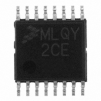
MCL908QY2CDTE Freescale Semiconductor, MCL908QY2CDTE Datasheet - Page 132

MCL908QY2CDTE
Manufacturer Part Number
MCL908QY2CDTE
Description
IC MCU 8BIT 1.5K FLASH 16-TSSOP
Manufacturer
Freescale Semiconductor
Series
HC08r
Datasheet
1.MCL908QY2CDWE.pdf
(182 pages)
Specifications of MCL908QY2CDTE
Core Processor
HC08
Core Size
8-Bit
Speed
2MHz
Peripherals
LVD, POR, PWM
Number Of I /o
13
Program Memory Size
1.5KB (1.5K x 8)
Program Memory Type
FLASH
Ram Size
128 x 8
Voltage - Supply (vcc/vdd)
2.4 V ~ 3.6 V
Data Converters
A/D 4x8b
Oscillator Type
Internal
Operating Temperature
-40°C ~ 85°C
Package / Case
16-TSSOP
Lead Free Status / RoHS Status
Lead free / RoHS Compliant
Eeprom Size
-
Connectivity
-
- Current page: 132 of 182
- Download datasheet (2Mb)
Timer Interface Module (TIM)
TOVx — Toggle-On-Overflow Bit
CHxMAX — Channel x Maximum Duty Cycle Bit
14.9.5 TIM Channel Registers
These read/write registers contain the captured TIM counter value of the input capture function or the
output compare value of the output compare function. The state of the TIM channel registers after reset
is unknown.
In input capture mode (MSxB:MSxA = 0:0), reading the high byte of the TIM channel x registers (TCHxH)
inhibits input captures until the low byte (TCHxL) is read.
In output compare mode (MSxB:MSxA ≠ 0:0), writing to the high byte of the TIM channel x registers
(TCHxH) inhibits output compares until the low byte (TCHxL) is written.
132
When ELSxB and ELSxA are both clear, channel x is not connected to an I/O port, and pin TCHx is
available as a general-purpose I/O pin.
the ELSxB and ELSxA bits.
When channel x is an output compare channel, this read/write bit controls the behavior of the channel
x output when the TIM counter overflows. When channel x is an input capture channel, TOVx has no
effect. Reset clears the TOVx bit.
When the TOVx bit is a 1, setting the CHxMAX bit forces the duty cycle of buffered and unbuffered
PWM signals to 100%. As
or cleared. The output stays at the 100% duty cycle level until the cycle after CHxMAX is cleared.
1 = Channel x pin toggles on TIM counter overflow.
0 = Channel x pin does not toggle on TIM counter overflow.
After initially enabling a TIM channel register for input capture operation
and selecting the edge sensitivity, clear CHxF to ignore any erroneous
edge detection flags.
When TOVx is set, a TIM counter overflow takes precedence over a
channel x output compare if both occur at the same time.
CHxMAX
TCHx
OVERFLOW
COMPARE
Figure 14-8
PERIOD
OUTPUT
MC68HLC908QY/QT Family Data Sheet, Rev. 3
OVERFLOW
Figure 14-8. CHxMAX Latency
shows, the CHxMAX bit takes effect in the cycle after it is set
Table 14-3
COMPARE
OUTPUT
NOTE
NOTE
OVERFLOW
shows how ELSxB and ELSxA work. Reset clears
COMPARE
OUTPUT
OVERFLOW
COMPARE
OUTPUT
OVERFLOW
Freescale Semiconductor
Related parts for MCL908QY2CDTE
Image
Part Number
Description
Manufacturer
Datasheet
Request
R
Part Number:
Description:
Manufacturer:
Freescale Semiconductor, Inc
Datasheet:
Part Number:
Description:
Manufacturer:
Freescale Semiconductor, Inc
Datasheet:
Part Number:
Description:
Manufacturer:
Freescale Semiconductor, Inc
Datasheet:
Part Number:
Description:
Manufacturer:
Freescale Semiconductor, Inc
Datasheet:
Part Number:
Description:
Manufacturer:
Freescale Semiconductor, Inc
Datasheet:
Part Number:
Description:
Manufacturer:
Freescale Semiconductor, Inc
Datasheet:
Part Number:
Description:
Manufacturer:
Freescale Semiconductor, Inc
Datasheet:
Part Number:
Description:
Manufacturer:
Freescale Semiconductor, Inc
Datasheet:
Part Number:
Description:
Manufacturer:
Freescale Semiconductor, Inc
Datasheet:
Part Number:
Description:
Manufacturer:
Freescale Semiconductor, Inc
Datasheet:
Part Number:
Description:
Manufacturer:
Freescale Semiconductor, Inc
Datasheet:
Part Number:
Description:
Manufacturer:
Freescale Semiconductor, Inc
Datasheet:
Part Number:
Description:
Manufacturer:
Freescale Semiconductor, Inc
Datasheet:
Part Number:
Description:
Manufacturer:
Freescale Semiconductor, Inc
Datasheet:
Part Number:
Description:
Manufacturer:
Freescale Semiconductor, Inc
Datasheet:


