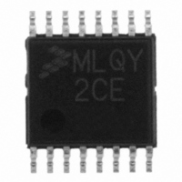
MCL908QY2CDTE Freescale Semiconductor, MCL908QY2CDTE Datasheet - Page 43

MCL908QY2CDTE
Manufacturer Part Number
MCL908QY2CDTE
Description
IC MCU 8BIT 1.5K FLASH 16-TSSOP
Manufacturer
Freescale Semiconductor
Series
HC08r
Datasheet
1.MCL908QY2CDWE.pdf
(182 pages)
Specifications of MCL908QY2CDTE
Core Processor
HC08
Core Size
8-Bit
Speed
2MHz
Peripherals
LVD, POR, PWM
Number Of I /o
13
Program Memory Size
1.5KB (1.5K x 8)
Program Memory Type
FLASH
Ram Size
128 x 8
Voltage - Supply (vcc/vdd)
2.4 V ~ 3.6 V
Data Converters
A/D 4x8b
Oscillator Type
Internal
Operating Temperature
-40°C ~ 85°C
Package / Case
16-TSSOP
Lead Free Status / RoHS Status
Lead free / RoHS Compliant
Eeprom Size
-
Connectivity
-
- Current page: 43 of 182
- Download datasheet (2Mb)
3.6 Input/Output Signals
The ADC module has four channels that are shared with I/O port A.
ADC voltage in (ADCVIN) is the input voltage signal from one of the four ADC channels to the ADC
module.
3.7 Input/Output Registers
These I/O registers control and monitor ADC operation:
3.7.1 ADC Status and Control Register
The following paragraphs describe the function of the ADC status and control register (ADSCR). When a
conversion is in process and the ADSCR is written, the current conversion data should be discarded to
prevent an incorrect reading.
COCO — Conversions Complete Bit
AIEN — ADC Interrupt Enable Bit
ADCO — ADC Continuous Conversion Bit
Freescale Semiconductor
•
•
•
In non-interrupt mode (AIEN = 0), COCO is a read-only bit that is set at the end of each conversion.
COCO will stay set until cleared by a read of the ADC data register. Reset clears this bit.
In interrupt mode (AIEN = 1), COCO is a read-only bit that is not set at the end of a conversion. It
always reads as a 0.
When this bit is set, an interrupt is generated at the end of an ADC conversion. The interrupt signal is
cleared when ADR is read or ADSCR is written. Reset clears the AIEN bit.
When set, the ADC will convert samples continuously and update ADR at the end of each conversion.
Only one conversion is allowed when this bit is cleared. Reset clears the ADCO bit.
1 = Conversion completed (AIEN = 0)
0 = Conversion not completed (AIEN = 0) or CPU interrupt enabled (AIEN = 1)
1 = ADC interrupt enabled
0 = ADC interrupt disabled
1 = Continuous ADC conversion
0 = One ADC conversion
ADC status and control register (ADSCR)
ADC data register (ADR)
ADC clock register (ADICLK)
Address: $003C
The write function of the COCO bit is reserved. When writing to the ADSCR
register, always have a 0 in the COCO bit position.
Reset:
Read:
Write:
COCO
Figure 3-3. ADC Status and Control Register (ADSCR)
Bit 7
R
R
0
= Reserved
MC68HLC908QY/QT Family Data Sheet, Rev. 3
AIEN
6
0
ADCO
5
0
NOTE
CH4
4
1
CH3
3
1
CH2
2
1
CH1
1
1
Input/Output Signals
Bit 0
CH0
1
43
Related parts for MCL908QY2CDTE
Image
Part Number
Description
Manufacturer
Datasheet
Request
R
Part Number:
Description:
Manufacturer:
Freescale Semiconductor, Inc
Datasheet:
Part Number:
Description:
Manufacturer:
Freescale Semiconductor, Inc
Datasheet:
Part Number:
Description:
Manufacturer:
Freescale Semiconductor, Inc
Datasheet:
Part Number:
Description:
Manufacturer:
Freescale Semiconductor, Inc
Datasheet:
Part Number:
Description:
Manufacturer:
Freescale Semiconductor, Inc
Datasheet:
Part Number:
Description:
Manufacturer:
Freescale Semiconductor, Inc
Datasheet:
Part Number:
Description:
Manufacturer:
Freescale Semiconductor, Inc
Datasheet:
Part Number:
Description:
Manufacturer:
Freescale Semiconductor, Inc
Datasheet:
Part Number:
Description:
Manufacturer:
Freescale Semiconductor, Inc
Datasheet:
Part Number:
Description:
Manufacturer:
Freescale Semiconductor, Inc
Datasheet:
Part Number:
Description:
Manufacturer:
Freescale Semiconductor, Inc
Datasheet:
Part Number:
Description:
Manufacturer:
Freescale Semiconductor, Inc
Datasheet:
Part Number:
Description:
Manufacturer:
Freescale Semiconductor, Inc
Datasheet:
Part Number:
Description:
Manufacturer:
Freescale Semiconductor, Inc
Datasheet:
Part Number:
Description:
Manufacturer:
Freescale Semiconductor, Inc
Datasheet:


