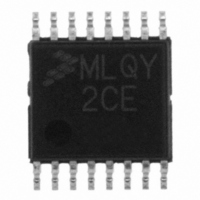
MCL908QY2CDTE Freescale Semiconductor, MCL908QY2CDTE Datasheet - Page 44

MCL908QY2CDTE
Manufacturer Part Number
MCL908QY2CDTE
Description
IC MCU 8BIT 1.5K FLASH 16-TSSOP
Manufacturer
Freescale Semiconductor
Series
HC08r
Datasheet
1.MCL908QY2CDWE.pdf
(182 pages)
Specifications of MCL908QY2CDTE
Core Processor
HC08
Core Size
8-Bit
Speed
2MHz
Peripherals
LVD, POR, PWM
Number Of I /o
13
Program Memory Size
1.5KB (1.5K x 8)
Program Memory Type
FLASH
Ram Size
128 x 8
Voltage - Supply (vcc/vdd)
2.4 V ~ 3.6 V
Data Converters
A/D 4x8b
Oscillator Type
Internal
Operating Temperature
-40°C ~ 85°C
Package / Case
16-TSSOP
Lead Free Status / RoHS Status
Lead free / RoHS Compliant
Eeprom Size
-
Connectivity
-
- Current page: 44 of 182
- Download datasheet (2Mb)
Analog-to-Digital Converter (ADC)
CH[4:0] — ADC Channel Select Bits
3.7.2 ADC Data Register
One 8-bit result register is provided. This register is updated each time an ADC conversion completes.
44
CH4, CH3, CH2, CH1, and CH0 form a 5-bit field which is used to select one of the four ADC channels.
The five select bits are detailed in
analog and a digital input simultaneously to prevent switching noise from corrupting the analog signal.
The ADC subsystem is turned off when the channel select bits are all set to 1. This feature allows for
reduced power consumption for the MCU when the ADC is not used. Reset sets all of these bits to a 1.
Address: $003E
Recovery from the disabled state requires one conversion cycle to stabilize.
Reset:
Read:
Write:
1. If any unused channels are selected, the resulting ADC conversion will be
2. The voltage levels supplied from internal reference nodes, as specified in the
CH4
↓
0
0
0
0
0
1
1
1
1
1
1
unknown.
table, are used to verify the operation of the ADC converter both in
production test and for user applications.
Bit 7
Bit 7
CH3
↓
0
0
0
0
0
1
1
1
1
1
1
MC68HLC908QY/QT Family Data Sheet, Rev. 3
Figure 3-4. ADC Data Register (ADR)
Bit 6
6
CH2
Table 3-1. MUX Channel Select
↓
0
0
0
0
1
0
0
1
1
1
1
Table
Bit 5
5
CH1
3-1. Care should be taken when using a port pin as both an
↓
0
0
1
1
0
1
1
0
0
1
1
Indeterminate after reset
NOTE
CH0
Bit 4
↓
4
0
1
0
1
0
0
1
0
1
0
1
Channel
Bit 3
ADC
AD0
AD1
AD2
AD3
3
—
—
—
—
—
—
—
—
Bit 2
2
ADC power off
Input Select
Unused
Reserved
Unused
V
V
PTA0
PTA1
PTA4
PTA5
DDA
SSA
Bit 1
(2)
(2)
1
(1)
Freescale Semiconductor
Bit 0
Bit 0
Related parts for MCL908QY2CDTE
Image
Part Number
Description
Manufacturer
Datasheet
Request
R
Part Number:
Description:
Manufacturer:
Freescale Semiconductor, Inc
Datasheet:
Part Number:
Description:
Manufacturer:
Freescale Semiconductor, Inc
Datasheet:
Part Number:
Description:
Manufacturer:
Freescale Semiconductor, Inc
Datasheet:
Part Number:
Description:
Manufacturer:
Freescale Semiconductor, Inc
Datasheet:
Part Number:
Description:
Manufacturer:
Freescale Semiconductor, Inc
Datasheet:
Part Number:
Description:
Manufacturer:
Freescale Semiconductor, Inc
Datasheet:
Part Number:
Description:
Manufacturer:
Freescale Semiconductor, Inc
Datasheet:
Part Number:
Description:
Manufacturer:
Freescale Semiconductor, Inc
Datasheet:
Part Number:
Description:
Manufacturer:
Freescale Semiconductor, Inc
Datasheet:
Part Number:
Description:
Manufacturer:
Freescale Semiconductor, Inc
Datasheet:
Part Number:
Description:
Manufacturer:
Freescale Semiconductor, Inc
Datasheet:
Part Number:
Description:
Manufacturer:
Freescale Semiconductor, Inc
Datasheet:
Part Number:
Description:
Manufacturer:
Freescale Semiconductor, Inc
Datasheet:
Part Number:
Description:
Manufacturer:
Freescale Semiconductor, Inc
Datasheet:
Part Number:
Description:
Manufacturer:
Freescale Semiconductor, Inc
Datasheet:


